NDS9933A Specs and Replacement
Type Designator: NDS9933A
Type of Transistor: MOSFET
Type of Control Channel: P-Channel
Absolute Maximum Ratings
Pd ⓘ
- Maximum Power Dissipation: 2 W
|Vds|ⓘ - Maximum Drain-Source Voltage: 20 V
|Id| ⓘ - Maximum Drain Current: 2.7 A
Tj ⓘ - Maximum Junction Temperature: 150 °C
Electrical Characteristics
|VGSth|ⓘ - Maximum Gate-Threshold Voltage: 4.5 V
Qg ⓘ - Total Gate Charge: 7.3 nC
RDSonⓘ - Maximum Drain-Source On-State Resistance: 0.14 Ohm
Package: SO8
- MOSFET ⓘ Cross-Reference Search
NDS9933A datasheet
..1. Size:853K cn vbsemi
nds9933a.pdf 
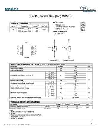
NDS9933A www.VBsemi.tw Dual P-Channel 30-V (D-S) MOSFET FEATURES PRODUCT SUMMARY Halogen-free VDS (V) RDS(on) ( ) ID (A)d, e Qg (Typ.) TrenchFET Power MOSFET 0.029 at VGS = - 10 V - 7.3 100 % UIS Tested RoHS - 30 17 nC COMPLIANT 0.039 at VGS = - 4.5 V - 6.3 APPLICATIONS Load Switches S1 S2 SO-8 S1 1 D1 8 G1 G2 G1 2 D1 7 S2 3 D2 6 G2 4 D2 5 Top Vie... See More ⇒
8.1. Size:211K fairchild semi
nds9936.pdf
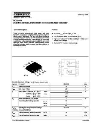
February 1996 NDS9936 Dual N-Channel Enhancement Mode Field Effect Transistor General Description Features These N-Channel enhancement mode power field effect 5A, 30V. RDS(ON) = 0.05 @ VGS = 10V. transistors are produced using Fairchild's proprietary, high cell High density cell design for extremely low RDS(ON). density, DMOS technology. This very high density process is especiall... See More ⇒
9.1. Size:258K fairchild semi
nds9948.pdf
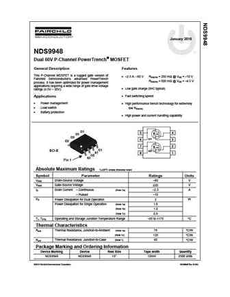
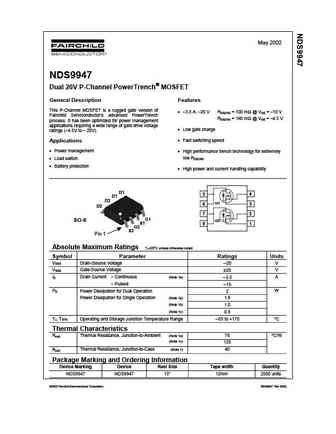
January 2010 NDS9948 Dual 60V P-Channel PowerTrench MOSFET General Description Features This P-Channel MOSFET is a rugged gate version of 2.3 A, 60 V RDS(ON) = 250 m @ VGS = 10 V Fairchild Semiconductor s advanced PowerTrench RDS(ON) = 500 m @ VGS = 4.5 V process. It has been optimized for power management applications requiring a wide ... See More ⇒
9.2. Size:209K fairchild semi
nds9956a.pdf
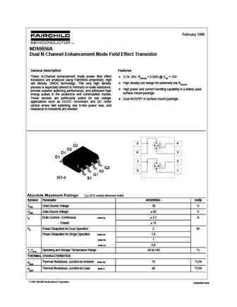
February 1996 NDS9956A Dual N-Channel Enhancement Mode Field Effect Transistor General Description Features These N-Channel enhancement mode power field effect 3.7A, 30V. RDS(ON) = 0.08 @ VGS = 10V transistors are produced using Fairchild's proprietary, high High density cell design for extremely low RDS(ON). cell density, DMOS technology. This very high density process is especia... See More ⇒
9.3. Size:210K fairchild semi
nds9953a.pdf
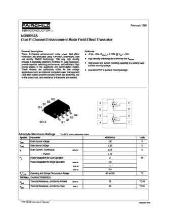
February 1996 NDS9953A Dual P-Channel Enhancement Mode Field Effect Transistor General Description Features These P-Channel enhancement mode power field effect -2.9A, -30V. RDS(ON) = 0.13 @ VGS = -10V. transistors are produced using Fairchild's proprietary, high High density cell design for extremely low RDS(ON). cell density, DMOS technology. This very high density process is espe... See More ⇒
9.4. Size:208K fairchild semi
nds9959.pdf
February 1996 NDS9959 Dual N-Channel Enhancement Mode Field Effect Transistor General Description Features These N-Channel enhancement mode power field effect 2.0A, 50V. RDS(ON) = 0.3 @ VGS = 10V transistors are produced using Fairchild's proprietary, high cell density, DMOS technology. This very high density process is High density cell design for extremely low RDS(ON). especially... See More ⇒
9.5. Size:77K fairchild semi
nds9945.pdf
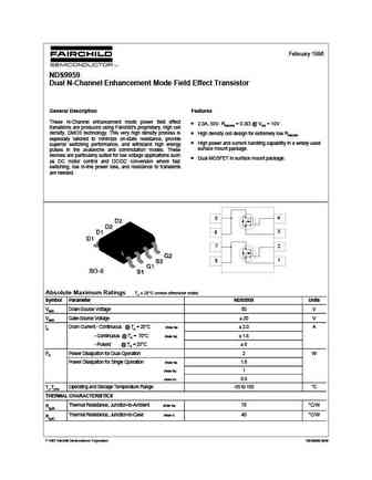
May 1998 NDS9945 Dual N-Channel Enhancement Mode Field Effect Transistor General Description Features SO-8 N-Channel enhancement mode power field effect 3.5 A, 60 V. RDS(ON) = 0.100 @ VGS = 10 V, transistors are produced using Fairchild's proprietary, high RDS(ON) = 0.200 @ VGS = 4.5 V. cell density, DMOS technology. This very high density process is especially tailored to ... See More ⇒
9.6. Size:141K fairchild semi
nds9947.pdf
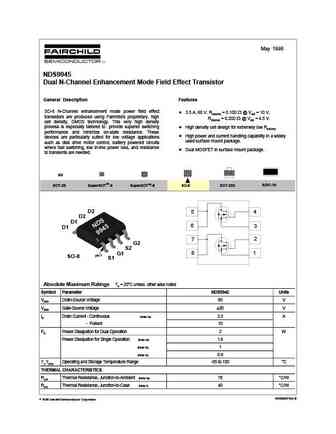
May 2002 NDS9947 Dual 20V P-Channel PowerTrench MOSFET General Description Features This P-Channel MOSFET is a rugged gate version of 3.5 A, 20 V RDS(ON) = 100 m @ VGS = 10 V Fairchild Semiconductor s advanced PowerTrench RDS(ON) = 190 m @ VGS = 4.5 V process. It has been optimized for power management applications requiring a wide ra... See More ⇒
9.7. Size:234K fairchild semi
nds9952a.pdf

February 1996 NDS9952A Dual N & P-Channel Enhancement Mode Field Effect Transistor General Description Features These dual N- and P-channel enhancement mode power N-Channel 3.7A, 30V, RDS(ON)=0.08 @ VGS=10V. field effect transistors are produced using Fairchild's P-Channel -2.9A, -30V, RDS(ON)=0.13 @ VGS=-10V. proprietary, high cell density, DMOS technology. This very high de... See More ⇒
9.8. Size:222K onsemi
nds9948.pdf
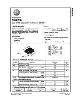
NDS9948 Dual 60V P-Channel PowerTrench MOSFET Features General Description This P-Channel MOSFET is a rugged gate version of 2.3 A, 60 V RDS(ON) = 250 m @ VGS = 10 V ON Semiconductor s advanced PowerTrench RDS(ON) = 500 m @ VGS = 4.5 V process. It has been optimized for power management Low gate charge (9nC typical) applications requi... See More ⇒
9.9. Size:915K cn vbsemi
nds9945-nl.pdf
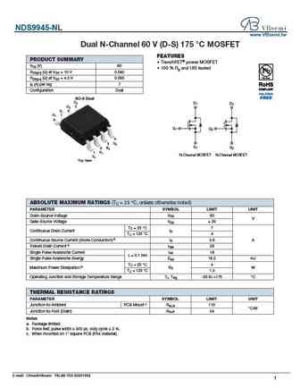
NDS9945-NL www.VBsemi.tw Dual N-Channel 60 V (D-S) 175 C MOSFET FEATURES PRODUCT SUMMARY TrenchFET power MOSFET VDS (V) 60 100 % Rg and UIS tested RDS(on) ( ) at VGS = 10 V 0.040 RDS(on) ( ) at VGS = 4.5 V 0.055 ID (A) per leg 7 Configuration Dual SO-8 Dual D2 D1 D2 D2 5 D1 6 D1 7 8 G1 G2 4 G2 3 3 S1 S2 S2 S2 2 2 G G1 1 1 N-Channel MOSFET N-Chann... See More ⇒
9.10. Size:868K cn vbsemi
nds9948-nl.pdf
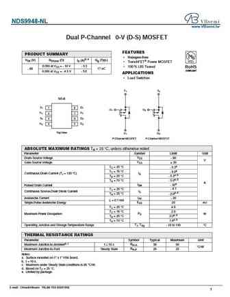
NDS9948-NL www.VBsemi.tw Dual P-Channel 6 0-V (D-S) MOSFET FEATURES PRODUCT SUMMARY Halogen-free VDS (V) RDS(on) ( ) ID (A)d, e Qg (Typ.) TrenchFET Power MOSFET 0.059 at VGS = - 10 V - 5.3 100 % UIS Tested RoHS - 60 17 nC COMPLIANT 0.069 at VGS = - 4.5 V - 5.0 APPLICATIONS Load Switches S1 S2 SO-8 S1 1 D1 8 G1 G2 G1 2 D1 7 S2 3 D2 6 G2 4 D2 5 Top ... See More ⇒
Detailed specifications: NDS8934
, NDS8936
, NDS8961
, NDS9400A
, NDS9407
, NDS9410A
, NDS9435A
, NDS9925A
, IRF9640
, NDS9936
, NDS9945
, NDS9947
, NDS9948
, NDS9953A
, NDS9955
, NDS9956A
, NDS9957
.
History: STH8NA60FI
Keywords - NDS9933A MOSFET specs
NDS9933A cross reference
NDS9933A equivalent finder
NDS9933A pdf lookup
NDS9933A substitution
NDS9933A replacement
Step-by-step guide to finding a MOSFET replacement. Cross-reference parts and ensure compatibility for your repair or project.
