CSD25213W10 Specs and Replacement
Type Designator: CSD25213W10
Type of Transistor: MOSFET
Type of Control Channel: P-Channel
Absolute Maximum Ratings
Pd ⓘ - Maximum Power Dissipation: 1 W
|Vds|ⓘ - Maximum Drain-Source Voltage: 20 V
|Vgs|ⓘ - Maximum Gate-Source Voltage: 6 V
|Id| ⓘ - Maximum Drain Current: 1.6 A
Tj ⓘ - Maximum Junction Temperature: 150 °C
Electrical Characteristics
tr ⓘ - Rise Time: 520 nS
Cossⓘ - Output Capacitance: 148 pF
RDSonⓘ - Maximum Drain-Source On-State Resistance: 0.047 Ohm
Package: DSBGA
CSD25213W10 substitution
- MOSFET ⓘ Cross-Reference Search
CSD25213W10 datasheet
csd25213w10.pdf
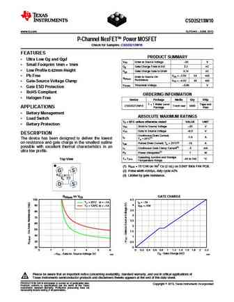
CSD25213W10 www.ti.com SLPS443 JUNE 2013 P-Channel NexFET Power MOSFET Check for Samples CSD25213W10 1 FEATURES PRODUCT SUMMARY Ultra Low Qg and Qgd VDS Drain to Source Voltage 20 V Small Footprint 1mm 1mm Qg Gate Charge Total (4.5V) 2.2 nC Low Profile 0.62mm Height Qgd Gate Charge Gate to Drain 0.14 nC VGS = 2.5V 54 m Pb Free RDS(on) Drain to S... See More ⇒
csd25211w1015.pdf
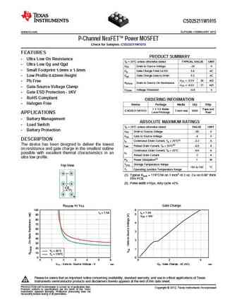
CSD25211W1015 www.ti.com SLPS296 FEBRUARY 2012 P-Channel NexFET Power MOSFET Check for Samples CSD25211W1015 1 FEATURES PRODUCT SUMMARY Ultra Low On Resistance TA = 25 C unless otherwise stated TYPICAL VALUE UNIT Ultra Low Qg and Qgd VDS Drain to Source Voltage -20 V Small Footprint 1.0mm x 1.5mm Qg Gate Charge Total (-4.5V) 3.4 nC Qgd Gate Charge Gate to Drain ... See More ⇒
csd25202w15.pdf
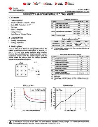
Sample & Support & Product Technical Tools & Buy Community Folder Documents Software CSD25202W15 SLPS508A JUNE 2014 REVISED JULY 2014 CSD25202W15 20-V P-Channel NexFET Power MOSFET 1 Features Product Summary 1 Low-Resistance TA = 25 C TYPICAL VALUE UNIT Small Footprint 1.5 mm 1.5 mm VDS Drain-to-Source Voltage 20 V Gate ESD Protection 3 kV Qg Gate C... See More ⇒
csd25201w15.pdf
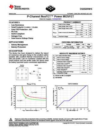
CSD25201W15 www.ti.com SLPS269A JUNE 2010 REVISED JULY 2011 P-Channel NexFET Power MOSFET Check for Samples CSD25201W15 PRODUCT SUMMARY 1 FEATURES VDS Drain to Drain Voltage 20 V Low Resistance Qg Gate Charge Total ( 4.5V) 4.3 nC Small Footprint 1.5-mm 1.5-mm Qgd Gate Charge Gate to Drain 0.7 nC Gate ESD Protection 3kV VGS = 1.8V 52 m Pb F... See More ⇒
Detailed specifications: CSD23201W10, CSD23202W10, CSD23203W, CSD23381F4, CSD23382F4, CSD25201W15, CSD25202W15, CSD25211W1015, STP75NF75, CSD25301W1015, CSD25302Q2, CSD25303W1015, CSD25304W1015, CSD25310Q2, CSD25401Q3, CSD25402Q3A, CSD25404Q3
Keywords - CSD25213W10 MOSFET specs
CSD25213W10 cross reference
CSD25213W10 equivalent finder
CSD25213W10 pdf lookup
CSD25213W10 substitution
CSD25213W10 replacement
Step-by-step guide to finding a MOSFET replacement. Cross-reference parts and ensure compatibility for your repair or project.
History: APT10M07JVFR | AOT8N50
🌐 : EN ES РУ

LIST
Last Update
MOSFET: FTF30P35D | FTF25N35DHVT | FTF15N35D | FTE15C35G | FTP02P15G | FTE02P15G | AKF30N5P0SX | AKF30N10S | AKF20P45D | CM4407
Popular searches
2sc3883 | c3306 datasheet | hy3810 | c711 transistor | k3599 transistor datasheet | 2sc1735 | transistor 2sc5200 | 2sb560 transistor