NVD3055-094 Datasheet. Specs and Replacement
Type Designator: NVD3055-094 📄📄
Type of Transistor: MOSFET
Type of Control Channel: N-Channel
Absolute Maximum Ratings
Pd ⓘ - Maximum Power Dissipation: 48 W
|Vds|ⓘ - Maximum Drain-Source Voltage: 60 V
|Vgs|ⓘ - Maximum Gate-Source Voltage: 20 V
|Id| ⓘ - Maximum Drain Current: 12 A
Tj ⓘ - Maximum Junction Temperature: 175 °C
Electrical Characteristics
tr ⓘ - Rise Time: 32.3 nS
Cossⓘ - Output Capacitance: 107 pF
RDSonⓘ - Maximum Drain-Source On-State Resistance: 0.094 Ohm
Package: DPAK
NVD3055-094 substitution
- MOSFET ⓘ Cross-Reference Search
NVD3055-094 datasheet
nvd3055-094.pdf
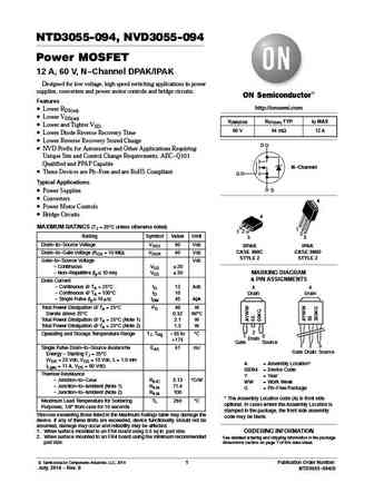
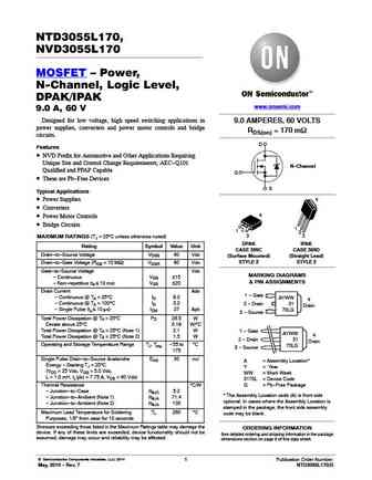
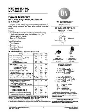
NTD3055-094, NVD3055-094 Power MOSFET 12 A, 60 V, N-Channel DPAK/IPAK Designed for low voltage, high speed switching applications in power supplies, converters and power motor controls and bridge circuits. Features http //onsemi.com Lower RDS(on) Lower VDS(on) V(BR)DSS RDS(on) TYP ID MAX Lower and Tighter VSD 60 V 94 mW 12 A Lower Diode Reverse Recovery Time Low... See More ⇒
ntd3055-094 nvd3055-094.pdf
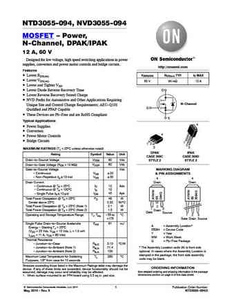
NTD3055-094, NVD3055-094 MOSFET Power, N-Channel, DPAK/IPAK 12 A, 60 V Designed for low voltage, high speed switching applications in power supplies, converters and power motor controls and bridge circuits. http //onsemi.com Features V(BR)DSS RDS(on) TYP ID MAX Lower RDS(on) Lower VDS(on) 60 V 94 mW 12 A Lower and Tighter VSD Lower Diode Reverse Recovery Time D ... See More ⇒
ntd3055-150 nvd3055-150.pdf
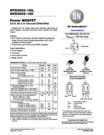
NTD3055-150, NVD3055-150 Power MOSFET 9.0 A, 60 V, N-Channel DPAK/IPAK Designed for low voltage, high speed switching applications in power supplies, converters and power motor controls and bridge www.onsemi.com circuits. 9.0 AMPERES, 60 VOLTS Features RDS(on) = 122 mW (Typ) NVD Prefix for Automotive and Other Applications Requiring D Unique Site and Control Change Requirements... See More ⇒
nvd3055-150.pdf
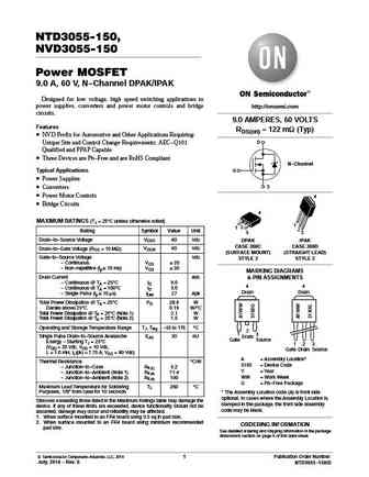
NTD3055-150, NVD3055-150 Power MOSFET 9.0 A, 60 V, N-Channel DPAK/IPAK Designed for low voltage, high speed switching applications in power supplies, converters and power motor controls and bridge http //onsemi.com circuits. 9.0 AMPERES, 60 VOLTS Features RDS(on) = 122 mW (Typ) NVD Prefix for Automotive and Other Applications Requiring D Unique Site and Control Change Requireme... See More ⇒
Detailed specifications: NVB5860NL, NVB60N06, NVB6410AN, NVB6411AN, NVB6412AN, NVB6413AN, NVD14N03R, NVD20N03L27, IRF520, NVD3055-150, NVD3055L170, NVD4804N, NVD4805N, NVD4806N, NVD4808N, NVD4809N, NVD4810N
Keywords - NVD3055-094 MOSFET specs
NVD3055-094 cross reference
NVD3055-094 equivalent finder
NVD3055-094 pdf lookup
NVD3055-094 substitution
NVD3055-094 replacement
Can't find your MOSFET? Learn how to find a substitute transistor by analyzing voltage, current and package compatibility
History: IXTP10P50P
🌐 : EN ES РУ
LIST
Last Update
MOSFET: ASDM30DN30E | ASDM3050KQ | ASDM2305 | ASDM2301 | ASDM2300ZA | ASDM20P13S | ASDM20N90Q | ASDM20N60 | ASDM7002EZA | ASDM68N80KQ
Popular searches
mp1620 transistor equivalent | 2sc945 transistor | c2073 transistor | ac176 transistor | mpsa20 | irfp264 | ksc2690 | bc546 datasheet
