NVD4810N Datasheet. Specs and Replacement
Type Designator: NVD4810N
Type of Transistor: MOSFET
Type of Control Channel: N-Channel
Absolute Maximum Ratings
Pd ⓘ
- Maximum Power Dissipation: 50 W
|Vds|ⓘ - Maximum Drain-Source Voltage: 30 V
|Vgs|ⓘ - Maximum Gate-Source Voltage: 20 V
|Id| ⓘ - Maximum Drain Current: 54 A
Tj ⓘ - Maximum Junction Temperature: 175 °C
Electrical Characteristics
tr ⓘ - Rise Time: 20.7 nS
Cossⓘ -
Output Capacitance: 284 pF
RDSonⓘ - Maximum Drain-Source On-State Resistance: 0.01 Ohm
Package: DPAK
- MOSFET ⓘ Cross-Reference Search
NVD4810N datasheet
..1. Size:148K onsemi
ntd4810n-1g nvd4810n.pdf 
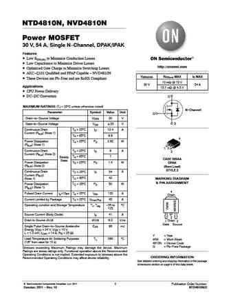
NTD4810N, NVD4810N Power MOSFET 30 V, 54 A, Single N-Channel, DPAK/IPAK Features Low RDS(on) to Minimize Conduction Losses Low Capacitance to Minimize Driver Losses http //onsemi.com Optimized Gate Charge to Minimize Switching Losses AEC-Q101 Qualified and PPAP Capable - NVD4810N V(BR)DSS RDS(on) MAX ID MAX These Devices are Pb-Free and are RoHS Compliant 10 mW @ ... See More ⇒
8.2. Size:108K onsemi
nvd4813nh.pdf
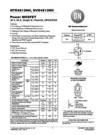
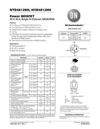
NTD4813NH, NVD4813NH Power MOSFET 30 V, 40 A, Single N-Channel, DPAK/IPAK Features Low RDS(on) to Minimize Conduction Losses Low Capacitance to Minimize Driver Losses http //onsemi.com Optimized Gate Charge to Minimize Switching Losses Low RG V(BR)DSS RDS(ON) MAX ID MAX NVD Prefix for Automotive and Other Applications Requiring 13 mW @ 10 V Unique Site and Contro... See More ⇒
9.1. Size:114K onsemi
nvd4806n.pdf
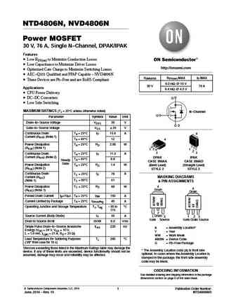
NTD4806N, NVD4806N Power MOSFET 30 V, 76 A, Single N-Channel, DPAK/IPAK Features Low RDS(on) to Minimize Conduction Losses Low Capacitance to Minimize Driver Losses http //onsemi.com Optimized Gate Charge to Minimize Switching Losses AEC-Q101 Qualified and PPAP Capable - NVD4806N V(BR)DSS RDS(on) MAX ID MAX These Devices are Pb-Free and are RoHS Compliant 6.0 mW @... See More ⇒
9.2. Size:113K onsemi
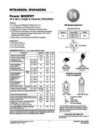
nvd4809n.pdf
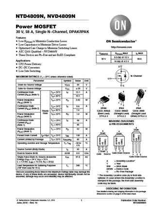
NTD4809N, NVD4809N Power MOSFET 30 V, 58 A, Single N-Channel, DPAK/IPAK Features Low RDS(on) to Minimize Conduction Losses Low Capacitance to Minimize Driver Losses http //onsemi.com Optimized Gate Charge to Minimize Switching Losses AEC Q101 Qualified - NVD4809N V(BR)DSS RDS(on) MAX ID MAX These Devices are Pb-Free and are RoHS Compliant 9.0 mW @ 10 V 30 V 58 A ... See More ⇒
9.3. Size:116K onsemi
ntd4805n nvd4805n.pdf

NTD4805N, NVD4805N Power MOSFET 30 V, 88 A, Single N-Channel, DPAK/IPAK Features Low RDS(on) to Minimize Conduction Losses Low Capacitance to Minimize Driver Losses http //onsemi.com Optimized Gate Charge to Minimize Switching Losses NVD Prefix for Automotive and Other Applications Requiring V(BR)DSS RDS(on) MAX ID MAX Unique Site and Control Change Requirements; AEC-Q... See More ⇒
9.4. Size:117K onsemi
ntd4809n nvd4809n.pdf

NTD4809N, NVD4809N Power MOSFET 30 V, 58 A, Single N-Channel, DPAK/IPAK Features Low RDS(on) to Minimize Conduction Losses Low Capacitance to Minimize Driver Losses http //onsemi.com Optimized Gate Charge to Minimize Switching Losses AEC Q101 Qualified - NVD4809N V(BR)DSS RDS(on) MAX ID MAX These Devices are Pb-Free and are RoHS Compliant 9.0 mW @ 10 V 30 V 58 A ... See More ⇒
9.5. Size:82K onsemi
nvd4804n.pdf
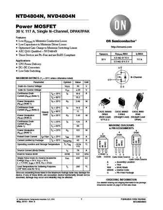
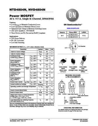
NTD4804N, NVD4804N Power MOSFET 30 V, 117 A, Single N-Channel, DPAK/IPAK Features Low RDS(on) to Minimize Conduction Losses Low Capacitance to Minimize Driver Losses http //onsemi.com Optimized Gate Charge to Minimize Switching Losses AEC Q101 Qualified - NVD4804N V(BR)DSS RDS(on) MAX ID MAX These Devices are Pb-Free and are RoHS Compliant 4.0 mW @ 10 V 30 V 117 ... See More ⇒
9.6. Size:113K onsemi
nvd4805n.pdf
NTD4805N, NVD4805N Power MOSFET 30 V, 88 A, Single N-Channel, DPAK/IPAK Features Low RDS(on) to Minimize Conduction Losses Low Capacitance to Minimize Driver Losses http //onsemi.com Optimized Gate Charge to Minimize Switching Losses NVD Prefix for Automotive and Other Applications Requiring V(BR)DSS RDS(on) MAX ID MAX Unique Site and Control Change Requirements; AEC-Q... See More ⇒
9.7. Size:112K onsemi
nvd4808n.pdf
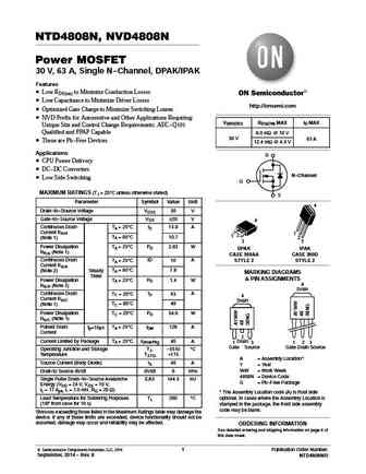
NTD4808N, NVD4808N Power MOSFET 30 V, 63 A, Single N-Channel, DPAK/IPAK Features Low RDS(on) to Minimize Conduction Losses Low Capacitance to Minimize Driver Losses http //onsemi.com Optimized Gate Charge to Minimize Switching Losses NVD Prefix for Automotive and Other Applications Requiring V(BR)DSS RDS(ON) MAX ID MAX Unique Site and Control Change Requirements; AEC-Q... See More ⇒
9.8. Size:115K onsemi
nvd4856n.pdf
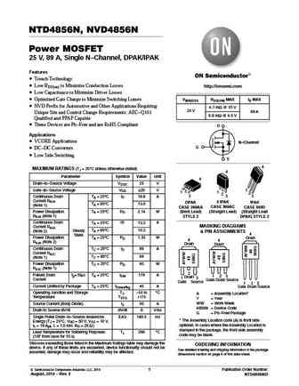
NTD4856N, NVD4856N Power MOSFET 25 V, 89 A, Single N-Channel, DPAK/IPAK Features Trench Technology Low RDS(on) to Minimize Conduction Losses http //onsemi.com Low Capacitance to Minimize Driver Losses Optimized Gate Charge to Minimize Switching Losses V(BR)DSS RDS(ON) MAX ID MAX NVD Prefix for Automotive and Other Applications Requiring 4.7 mW @ 10 V 25 V 89 A U... See More ⇒
9.9. Size:89K onsemi
ntd4804n nvd4804n.pdf
NTD4804N, NVD4804N Power MOSFET 30 V, 117 A, Single N-Channel, DPAK/IPAK Features Low RDS(on) to Minimize Conduction Losses Low Capacitance to Minimize Driver Losses www.onsemi.com Optimized Gate Charge to Minimize Switching Losses AEC Q101 Qualified - NVD4804N V(BR)DSS RDS(on) MAX ID MAX These Devices are Pb-Free and are RoHS Compliant 4.0 mW @ 10 V 30 V 117 A ... See More ⇒
Detailed specifications: NVD3055-094, NVD3055-150, NVD3055L170, NVD4804N, NVD4805N, NVD4806N, NVD4808N, NVD4809N, AO3400A, NVD4813NH, NVD4856N, NVD4C05N, NVD5117PL, NVD5414N, NVD5484NL, NVD5490NL, NVD5802N
Keywords - NVD4810N MOSFET specs
NVD4810N cross reference
NVD4810N equivalent finder
NVD4810N pdf lookup
NVD4810N substitution
NVD4810N replacement
Can't find your MOSFET?
Learn how to find a substitute transistor by analyzing voltage, current and package compatibility