BUK457-400B Specs and Replacement
Type Designator: BUK457-400B
Type of Transistor: MOSFET
Type of Control Channel: N-Channel
Absolute Maximum Ratings
Pd ⓘ
- Maximum Power Dissipation: 150 W
|Vds|ⓘ - Maximum Drain-Source Voltage: 400 V
|Vgs|ⓘ - Maximum Gate-Source Voltage: 30 V
|Id| ⓘ - Maximum Drain Current: 11 A
Tj ⓘ - Maximum Junction Temperature: 150 °C
Electrical Characteristics
tr ⓘ - Rise Time: 60 nS
Cossⓘ -
Output Capacitance: 170 pF
RDSonⓘ - Maximum Drain-Source On-State Resistance: 0.5 Ohm
Package: TO220AB
- MOSFET ⓘ Cross-Reference Search
BUK457-400B datasheet
4.2. Size:229K inchange semiconductor
buk457-400.pdf 

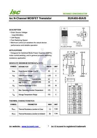
isc N-Channel MOSFET Transistor BUK457-400A/B DESCRIPTION Drain Source Voltage- V =400V(Min) DSS Low R DS(ON) Fast Switching Speed Minimum Lot-to-Lot variations for robust device performance and reliable operation APPLICATIONS Designed for Switched Mode Power Supplies (SMPS), motor control,welding, and in general purpose switching resistance application ABSOLUTE MAXIMU... See More ⇒
9.1. Size:54K philips
buk456-60a-b 1.pdf

Philips Semiconductors Product Specification PowerMOS transistor BUK456-60A/B GENERAL DESCRIPTION QUICK REFERENCE DATA N-channel enhancement mode SYMBOL PARAMETER MAX. MAX. UNIT field-effect power transistor in a plastic envelope. BUK456 -60A -60B The device is intended for use in VDS Drain-source voltage 60 60 V Switched Mode Power Supplies ID Drain current (DC) 52 51 A (SMPS), motor... See More ⇒
9.2. Size:57K philips
buk453-100a-b 2.pdf
Philips Semiconductors Product Specification PowerMOS transistor BUK453-100A/B GENERAL DESCRIPTION QUICK REFERENCE DATA N-channel enhancement mode SYMBOL PARAMETER MAX. MAX. UNIT field-effect power transistor in a plastic envelope. BUK453 -100A -100B The device is intended for use in VDS Drain-source voltage 100 100 V Switched Mode Power Supplies ID Drain current (DC) 14 13 A (SMPS), ... See More ⇒
9.3. Size:54K philips
buk452-60a-b.pdf

Philips Semiconductors Product Specification PowerMOS transistor BUK452-60A/B GENERAL DESCRIPTION QUICK REFERENCE DATA N-channel enhancement mode SYMBOL PARAMETER MAX. MAX. UNIT field-effect power transistor in a plastic envelope. BUK452 -60A -60B The device is intended for use in VDS Drain-source voltage 60 60 V Switched Mode Power Supplies ID Drain current (DC) 15 14 A (SMPS), motor... See More ⇒
9.4. Size:55K philips
buk456-100b.pdf
Philips Semiconductors Product specification PowerMOS transistor BUK456-100A/B GENERAL DESCRIPTION QUICK REFERENCE DATA N-channel enhancement mode SYMBOL PARAMETER MAX. MAX. UNIT field-effect power transistor in a plastic envelope. BUK456 -100A -100B The device is intended for use in VDS Drain-source voltage 100 100 V Switched Mode Power Supplies ID Drain current (DC) 34 32 A (SMPS), ... See More ⇒
9.5. Size:53K philips
buk456-100a-b 2.pdf

Philips Semiconductors Product specification PowerMOS transistor BUK456-100A/B GENERAL DESCRIPTION QUICK REFERENCE DATA N-channel enhancement mode SYMBOL PARAMETER MAX. MAX. UNIT field-effect power transistor in a plastic envelope. BUK456 -100A -100B The device is intended for use in VDS Drain-source voltage 100 100 V Switched Mode Power Supplies ID Drain current (DC) 34 32 A (SMPS), ... See More ⇒
9.6. Size:54K philips
buk455-200a-b 1.pdf
Philips Semiconductors Product Specification PowerMOS transistor BUK455-200A/B GENERAL DESCRIPTION QUICK REFERENCE DATA N-channel enhancement mode SYMBOL PARAMETER MAX. MAX. UNIT field-effect power transistor in a plastic envelope. BUK455 -200A -200B The device is intended for use in VDS Drain-source voltage 200 200 V Switched Mode Power Supplies ID Drain current (DC) 14 13 A (SMPS), ... See More ⇒
9.7. Size:64K philips
buk454-800a-b.pdf
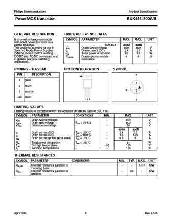
Philips Semiconductors Product Specification PowerMOS transistor BUK454-800A/B GENERAL DESCRIPTION QUICK REFERENCE DATA N-channel enhancement mode SYMBOL PARAMETER MAX. MAX. UNIT field-effect power transistor in a plastic envelope. BUK454 -800A -800B The device is intended for use in VDS Drain-source voltage 800 800 V Switched Mode Power Supplies ID Drain current (DC) 2.4 2.0 A (SMPS)... See More ⇒
9.8. Size:56K philips
buk452-100a-b 1.pdf

Philips Semiconductors Product Specification PowerMOS transistor BUK452-100A/B GENERAL DESCRIPTION QUICK REFERENCE DATA N-channel enhancement mode SYMBOL PARAMETER MAX. MAX. UNIT field-effect power transistor in a plastic envelope. BUK452 -100A -100B The device is intended for use in VDS Drain-source voltage 100 100 V Switched Mode Power Supplies ID Drain current (DC) 11 10 A (SMPS), ... See More ⇒
9.9. Size:54K philips
buk453-60a-b.pdf

Philips Semiconductors Product Specification PowerMOS transistor BUK453-60A/B GENERAL DESCRIPTION QUICK REFERENCE DATA N-channel enhancement mode SYMBOL PARAMETER MAX. MAX. UNIT field-effect power transistor in a plastic envelope. BUK453 -60A -60B The device is intended for use in VDS Drain-source voltage 60 60 V Switched Mode Power Supplies ID Drain current (DC) 22 20 A (SMPS), motor... See More ⇒
9.10. Size:54K philips
buk455-100a-b 1.pdf

Philips Semiconductors Product Specification PowerMOS transistor BUK455-100A/B GENERAL DESCRIPTION QUICK REFERENCE DATA N-channel enhancement mode SYMBOL PARAMETER MAX. MAX. UNIT field-effect power transistor in a plastic envelope. BUK455 -100A -100B The device is intended for use in VDS Drain-source voltage 100 100 V Switched Mode Power Supplies ID Drain current (DC) 26 23 A (SMPS), ... See More ⇒
9.11. Size:50K philips
buk456-200a-b 1.pdf

Philips Semiconductors Product Specification PowerMOS transistor BUK456-200A/B GENERAL DESCRIPTION QUICK REFERENCE DATA N-channel enhancement mode SYMBOL PARAMETER MAX. MAX. UNIT field-effect power transistor in a plastic envelope. BUK456 -200A -200B The device is intended for use in VDS Drain-source voltage 200 200 V Switched Mode Power Supplies ID Drain current (DC) 19 17 A (SMPS), ... See More ⇒
9.12. Size:71K philips
buk455-60h 1.pdf
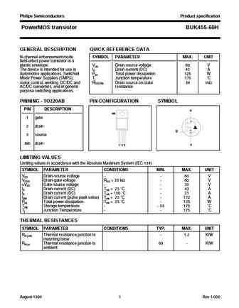
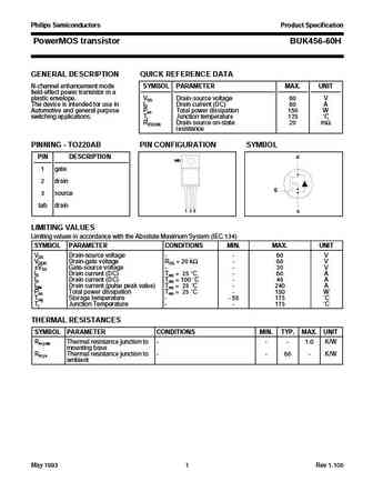
Philips Semiconductors Product specification PowerMOS transistor BUK455-60H GENERAL DESCRIPTION QUICK REFERENCE DATA N-channel enhancement mode SYMBOL PARAMETER MAX. UNIT field-effect power transistor in a plastic envelope. VDS Drain-source voltage 60 V The device is intended for use in ID Drain current (DC) 43 A Automotive applications, Switched Ptot Total power dissipation 125 W Mod... See More ⇒
9.13. Size:51K philips
buk454-60h 1.pdf
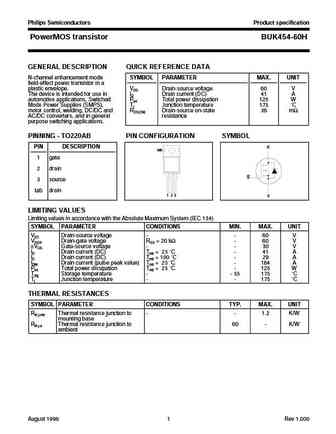
Philips Semiconductors Product specification PowerMOS transistor BUK454-60H GENERAL DESCRIPTION QUICK REFERENCE DATA N-channel enhancement mode SYMBOL PARAMETER MAX. UNIT field-effect power transistor in a plastic envelope. VDS Drain-source voltage 60 V The device is intended for use in ID Drain current (DC) 41 A automotive applications, Switched Ptot Total power dissipation 125 W Mod... See More ⇒
9.14. Size:49K philips
buk456-800a-b.pdf

Philips Semiconductors Product Specification PowerMOS transistor BUK456-800A/B GENERAL DESCRIPTION QUICK REFERENCE DATA N-channel enhancement mode SYMBOL PARAMETER MAX. MAX. UNIT field-effect power transistor in a plastic envelope. BUK456 -800A -800B The device is intended for use in VDS Drain-source voltage 800 800 V Switched Mode Power Supplies ID Drain current (DC) 4 3.5 A (SMPS), ... See More ⇒
9.15. Size:58K philips
buk454-200a-b 1.pdf
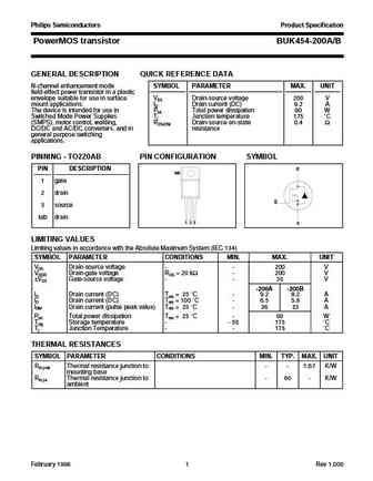
Philips Semiconductors Product Specification PowerMOS transistor BUK454-200A/B GENERAL DESCRIPTION QUICK REFERENCE DATA N-channel enhancement mode SYMBOL PARAMETER MAX. UNIT field-effect power transistor in a plastic envelope suitable for use in surface VDS Drain-source voltage 200 V mount applications. ID Drain current (DC) 9.2 A The device is intended for use in Ptot Total power diss... See More ⇒
9.16. Size:48K philips
buk451-100a-b 1.pdf
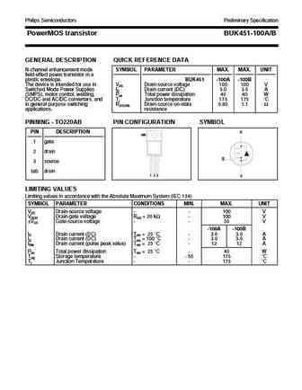
Philips Semiconductors Preliminary Specification PowerMOS transistor BUK451-100A/B GENERAL DESCRIPTION QUICK REFERENCE DATA N-channel enhancement mode SYMBOL PARAMETER MAX. MAX. UNIT field-effect power transistor in a plastic envelope. BUK451 -100A -100B The device is intended for use in VDS Drain-source voltage 100 100 V Switched Mode Power Supplies ID Drain current (DC) 3.0 3.0 A (S... See More ⇒
9.17. Size:67K philips
buk456-60a-b 2.pdf

Philips Semiconductors Product Specification PowerMOS transistor BUK456-60A/B GENERAL DESCRIPTION QUICK REFERENCE DATA N-channel enhancement mode SYMBOL PARAMETER MAX. MAX. UNIT field-effect power transistor in a plastic envelope. BUK456 -60A -60B The device is intended for use in VDS Drain-source voltage 60 60 V Switched Mode Power Supplies ID Drain current (DC) 52 51 A (SMPS), motor... See More ⇒
9.18. Size:53K philips
buk455-200b.pdf

Philips Semiconductors Product Specification PowerMOS transistor BUK455-200A/B GENERAL DESCRIPTION QUICK REFERENCE DATA N-channel enhancement mode SYMBOL PARAMETER MAX. MAX. UNIT field-effect power transistor in a plastic envelope. BUK455 -200A -200B The device is intended for use in VDS Drain-source voltage 200 200 V Switched Mode Power Supplies ID Drain current (DC) 14 13 A (SMPS), ... See More ⇒
9.19. Size:79K philips
buk455.pdf

Philips Semiconductors Product Specification PowerMOS transistor BUK455-60A/B GENERAL DESCRIPTION QUICK REFERENCE DATA N-channel enhancement mode SYMBOL PARAMETER MAX. MAX. UNIT field-effect power transistor in a plastic envelope. BUK455 -60A -60B The device is intended for use in VDS Drain-source voltage 60 60 V Switched Mode Power Supplies ID Drain current (DC) 41 38 A (SMPS), motor... See More ⇒
9.20. Size:57K philips
buk456-60h 1.pdf
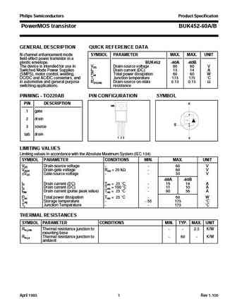
Philips Semiconductors Product Specification PowerMOS transistor BUK456-60H GENERAL DESCRIPTION QUICK REFERENCE DATA N-channel enhancement mode SYMBOL PARAMETER MAX. UNIT field-effect power transistor in a plastic envelope. VDS Drain-source voltage 60 V The device is intended for use in ID Drain current (DC) 60 A Automotive and general purpose Ptot Total power dissipation 150 W switch... See More ⇒
9.21. Size:61K philips
buk452-100b.pdf

Philips Semiconductors Product Specification PowerMOS transistor BUK452-100A/B GENERAL DESCRIPTION QUICK REFERENCE DATA N-channel enhancement mode SYMBOL PARAMETER MAX. MAX. UNIT field-effect power transistor in a plastic envelope. BUK452 -100A -100B The device is intended for use in VDS Drain-source voltage 100 100 V Switched Mode Power Supplies ID Drain current (DC) 11 10 A (SMPS), ... See More ⇒
9.22. Size:56K philips
buk455-60a-b 1.pdf

Philips Semiconductors Product Specification PowerMOS transistor BUK455-60A/B GENERAL DESCRIPTION QUICK REFERENCE DATA N-channel enhancement mode SYMBOL PARAMETER MAX. MAX. UNIT field-effect power transistor in a plastic envelope. BUK455 -60A -60B The device is intended for use in VDS Drain-source voltage 60 60 V Switched Mode Power Supplies ID Drain current (DC) 41 38 A (SMPS), motor... See More ⇒
9.23. Size:54K philips
buk452-60a-b 1.pdf
Philips Semiconductors Product Specification PowerMOS transistor BUK452-60A/B GENERAL DESCRIPTION QUICK REFERENCE DATA N-channel enhancement mode SYMBOL PARAMETER MAX. MAX. UNIT field-effect power transistor in a plastic envelope. BUK452 -60A -60B The device is intended for use in VDS Drain-source voltage 60 60 V Switched Mode Power Supplies ID Drain current (DC) 15 14 A (SMPS), motor... See More ⇒
9.24. Size:54K philips
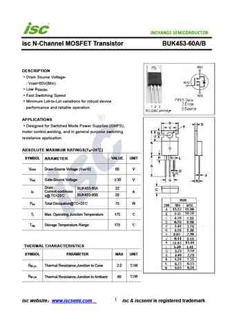
buk453-60a-b 1.pdf

Philips Semiconductors Product Specification PowerMOS transistor BUK453-60A/B GENERAL DESCRIPTION QUICK REFERENCE DATA N-channel enhancement mode SYMBOL PARAMETER MAX. MAX. UNIT field-effect power transistor in a plastic envelope. BUK453 -60A -60B The device is intended for use in VDS Drain-source voltage 60 60 V Switched Mode Power Supplies ID Drain current (DC) 22 20 A (SMPS), motor... See More ⇒
9.25. Size:56K philips
buk455-60a-b.pdf

Philips Semiconductors Product Specification PowerMOS transistor BUK455-60A/B GENERAL DESCRIPTION QUICK REFERENCE DATA N-channel enhancement mode SYMBOL PARAMETER MAX. MAX. UNIT field-effect power transistor in a plastic envelope. BUK455 -60A -60B The device is intended for use in VDS Drain-source voltage 60 60 V Switched Mode Power Supplies ID Drain current (DC) 41 38 A (SMPS), motor... See More ⇒
9.26. Size:48K philips
buk455-100b.pdf

Philips Semiconductors Product Specification PowerMOS transistor BUK455-100A/B GENERAL DESCRIPTION QUICK REFERENCE DATA N-channel enhancement mode SYMBOL PARAMETER MAX. MAX. UNIT field-effect power transistor in a plastic envelope. BUK455 -100A -100B The device is intended for use in VDS Drain-source voltage 100 100 V Switched Mode Power Supplies ID Drain current (DC) 26 23 A (SMPS), ... See More ⇒
9.27. Size:228K inchange semiconductor
buk456-100.pdf

isc N-Channel MOSFET Transistor BUK456-100A/B DESCRIPTION Drain Source Voltage- V =100V(Min) DSS Low R DS(ON) Fast Switching Speed Minimum Lot-to-Lot variations for robust device performance and reliable operation APPLICATIONS Designed for Switched Mode Power Supplies (SMPS), motor control,welding, and in general purpose switching resistance application ABSOLUTE MAXIMU... See More ⇒
9.28. Size:229K inchange semiconductor
buk455-60.pdf
isc N-Channel MOSFET Transistor BUK455-60A/B DESCRIPTION Drain Source Voltage- V =60V(Min) DSS Low R DS(ON) Fast Switching Speed Minimum Lot-to-Lot variations for robust device performance and reliable operation APPLICATIONS Designed for Switched Mode Power Supplies (SMPS), motor control,welding, and in general purpose switching resistance application ABSOLUTE MAXIMUM ... See More ⇒
9.29. Size:229K inchange semiconductor
buk456-200.pdf

isc N-Channel MOSFET Transistor BUK456-200A/B DESCRIPTION Drain Source Voltage- V =200V(Min) DSS Low R DS(ON) Fast Switching Speed Minimum Lot-to-Lot variations for robust device performance and reliable operation APPLICATIONS Designed for Switched Mode Power Supplies (SMPS), motor control,welding, and in general purpose switching resistance application ABSOLUTE MAXIMU... See More ⇒
9.30. Size:228K inchange semiconductor
buk455-200.pdf

isc N-Channel MOSFET Transistor BUK455-200A/B DESCRIPTION Drain Source Voltage- V =200V(Min) DSS Low R DS(ON) Fast Switching Speed Minimum Lot-to-Lot variations for robust device performance and reliable operation APPLICATIONS Designed for Switched Mode Power Supplies (SMPS), motor control,welding, and in general purpose switching resistance application ABSOLUTE MAXIMU... See More ⇒
9.31. Size:228K inchange semiconductor
buk452-60.pdf

isc N-Channel MOSFET Transistor BUK452-60A/B DESCRIPTION Drain Source Voltage- V =60V(Min) DSS Low R DS(ON) Fast Switching Speed Minimum Lot-to-Lot variations for robust device performance and reliable operation APPLICATIONS Designed for Switched Mode Power Supplies (SMPS), motor control,welding, and in general purpose switching resistance application ABSOLUTE MAXIMUM ... See More ⇒
9.32. Size:228K inchange semiconductor
buk452-100.pdf

isc N-Channel MOSFET Transistor BUK452-100A/B DESCRIPTION Drain Source Voltage- V =100V(Min) DSS Low R DS(ON) Fast Switching Speed Minimum Lot-to-Lot variations for robust device performance and reliable operation APPLICATIONS Designed for Switched Mode Power Supplies (SMPS), motor control,welding, and in general purpose switching resistance application ABSOLUTE MAXIMU... See More ⇒
9.33. Size:228K inchange semiconductor
buk455-100.pdf
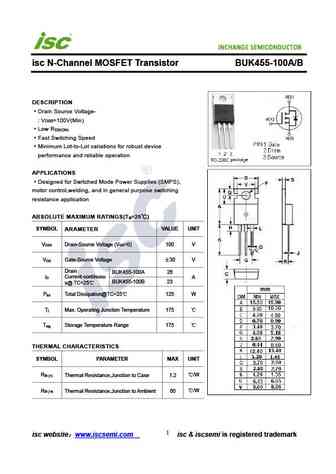
isc N-Channel MOSFET Transistor BUK455-100A/B DESCRIPTION Drain Source Voltage- V =100V(Min) DSS Low R DS(ON) Fast Switching Speed Minimum Lot-to-Lot variations for robust device performance and reliable operation APPLICATIONS Designed for Switched Mode Power Supplies (SMPS), motor control,welding, and in general purpose switching resistance application ABSOLUTE MAXIMU... See More ⇒
9.34. Size:229K inchange semiconductor
buk453-60.pdf
isc N-Channel MOSFET Transistor BUK453-60A/B DESCRIPTION Drain Source Voltage- V =60V(Min) DSS Low R DS(ON) Fast Switching Speed Minimum Lot-to-Lot variations for robust device performance and reliable operation APPLICATIONS Designed for Switched Mode Power Supplies (SMPS), motor control,welding, and in general purpose switching resistance application ABSOLUTE MAXIMUM ... See More ⇒
9.35. Size:229K inchange semiconductor
buk456-800.pdf
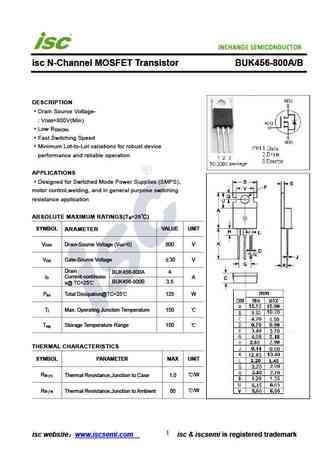
isc N-Channel MOSFET Transistor BUK456-800A/B DESCRIPTION Drain Source Voltage- V =800V(Min) DSS Low R DS(ON) Fast Switching Speed Minimum Lot-to-Lot variations for robust device performance and reliable operation APPLICATIONS Designed for Switched Mode Power Supplies (SMPS), motor control,welding, and in general purpose switching resistance application ABSOLUTE MAXIMU... See More ⇒
9.36. Size:229K inchange semiconductor
buk454-800.pdf

isc N-Channel MOSFET Transistor BUK454-800A/B DESCRIPTION Drain Source Voltage- V =800V(Min) DSS Low R DS(ON) Fast Switching Speed Minimum Lot-to-Lot variations for robust device performance and reliable operation APPLICATIONS Designed for Switched Mode Power Supplies (SMPS), motor control,welding, and in general purpose switching resistance application ABSOLUTE MAXIMU... See More ⇒
9.37. Size:228K inchange semiconductor
buk454-200.pdf

isc N-Channel MOSFET Transistor BUK454-200A/B DESCRIPTION Drain Source Voltage- V =200V(Min) DSS Low R DS(ON) Fast Switching Speed Minimum Lot-to-Lot variations for robust device performance and reliable operation APPLICATIONS Designed for Switched Mode Power Supplies (SMPS), motor control,welding, and in general purpose switching resistance application ABSOLUTE MAXIMU... See More ⇒
9.38. Size:228K inchange semiconductor
buk453-100.pdf
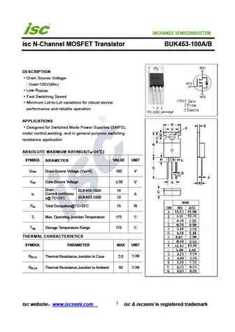
isc N-Channel MOSFET Transistor BUK453-100A/B DESCRIPTION Drain Source Voltage- V =100V(Min) DSS Low R DS(ON) Fast Switching Speed Minimum Lot-to-Lot variations for robust device performance and reliable operation APPLICATIONS Designed for Switched Mode Power Supplies (SMPS), motor control,welding, and in general purpose switching resistance application ABSOLUTE MAXIMU... See More ⇒
9.39. Size:229K inchange semiconductor
buk456-60.pdf

isc N-Channel MOSFET Transistor BUK456-60A/B DESCRIPTION Drain Source Voltage- V =60V(Min) DSS Low R DS(ON) Fast Switching Speed Minimum Lot-to-Lot variations for robust device performance and reliable operation APPLICATIONS Designed for Switched Mode Power Supplies (SMPS), motor control,welding, and in general purpose switching resistance application ABSOLUTE MAXIMUM ... See More ⇒
Detailed specifications: APT5014BFLLG, APT5014BLLG, APT5014LVFRG, APT5014SFLLG, APT5014SLLG, APT5015BVFRG, 2SK1982-01MR, BUK457-400A, IRFZ24N, 2SK125, 2SJ410, 2SK2518-01MR, 2SK4027, APT5016BFLLG, APT5016BLLG, APT5016SFLLG, APT5017SVFRG
Keywords - BUK457-400B MOSFET specs
BUK457-400B cross reference
BUK457-400B equivalent finder
BUK457-400B pdf lookup
BUK457-400B substitution
BUK457-400B replacement
Need a MOSFET replacement?
Our guide shows you how to find a perfect substitute by comparing key parameters and specs