BUK457-400B. Аналоги и основные параметры
Наименование производителя: BUK457-400B
Тип транзистора: MOSFET
Полярность: N
Предельные значения
Pd ⓘ
- Максимальная рассеиваемая мощность: 150 W
|Vds|ⓘ - Максимально допустимое напряжение сток-исток: 400 V
|Vgs|ⓘ - Максимально допустимое напряжение затвор-исток: 30 V
|Id| ⓘ - Максимально допустимый постоянный ток стока: 11 A
Tj ⓘ - Максимальная температура канала: 150 °C
Электрические характеристики
tr ⓘ -
Время нарастания: 60 ns
Cossⓘ - Выходная емкость: 170 pf
RDSonⓘ - Сопротивление сток-исток открытого транзистора: 0.5 Ohm
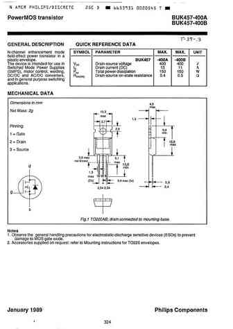
Тип корпуса: TO220AB
Аналог (замена) для BUK457-400B
- подборⓘ MOSFET транзистора по параметрам
BUK457-400B даташит
4.2. Size:229K inchange semiconductor
buk457-400.pdf 

isc N-Channel MOSFET Transistor BUK457-400A/B DESCRIPTION Drain Source Voltage- V =400V(Min) DSS Low R DS(ON) Fast Switching Speed Minimum Lot-to-Lot variations for robust device performance and reliable operation APPLICATIONS Designed for Switched Mode Power Supplies (SMPS), motor control,welding, and in general purpose switching resistance application ABSOLUTE MAXIMU
9.1. Size:54K philips
buk456-60a-b 1.pdf 
Philips Semiconductors Product Specification PowerMOS transistor BUK456-60A/B GENERAL DESCRIPTION QUICK REFERENCE DATA N-channel enhancement mode SYMBOL PARAMETER MAX. MAX. UNIT field-effect power transistor in a plastic envelope. BUK456 -60A -60B The device is intended for use in VDS Drain-source voltage 60 60 V Switched Mode Power Supplies ID Drain current (DC) 52 51 A (SMPS), motor
9.2. Size:57K philips
buk453-100a-b 2.pdf 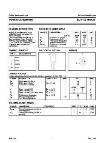
Philips Semiconductors Product Specification PowerMOS transistor BUK453-100A/B GENERAL DESCRIPTION QUICK REFERENCE DATA N-channel enhancement mode SYMBOL PARAMETER MAX. MAX. UNIT field-effect power transistor in a plastic envelope. BUK453 -100A -100B The device is intended for use in VDS Drain-source voltage 100 100 V Switched Mode Power Supplies ID Drain current (DC) 14 13 A (SMPS),
9.3. Size:54K philips
buk452-60a-b.pdf 
Philips Semiconductors Product Specification PowerMOS transistor BUK452-60A/B GENERAL DESCRIPTION QUICK REFERENCE DATA N-channel enhancement mode SYMBOL PARAMETER MAX. MAX. UNIT field-effect power transistor in a plastic envelope. BUK452 -60A -60B The device is intended for use in VDS Drain-source voltage 60 60 V Switched Mode Power Supplies ID Drain current (DC) 15 14 A (SMPS), motor
9.4. Size:55K philips
buk456-100b.pdf 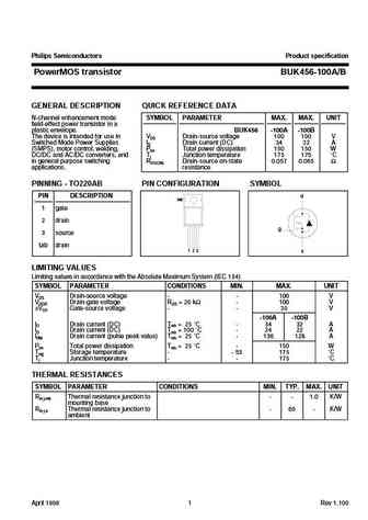
Philips Semiconductors Product specification PowerMOS transistor BUK456-100A/B GENERAL DESCRIPTION QUICK REFERENCE DATA N-channel enhancement mode SYMBOL PARAMETER MAX. MAX. UNIT field-effect power transistor in a plastic envelope. BUK456 -100A -100B The device is intended for use in VDS Drain-source voltage 100 100 V Switched Mode Power Supplies ID Drain current (DC) 34 32 A (SMPS),
9.5. Size:53K philips
buk456-100a-b 2.pdf 
Philips Semiconductors Product specification PowerMOS transistor BUK456-100A/B GENERAL DESCRIPTION QUICK REFERENCE DATA N-channel enhancement mode SYMBOL PARAMETER MAX. MAX. UNIT field-effect power transistor in a plastic envelope. BUK456 -100A -100B The device is intended for use in VDS Drain-source voltage 100 100 V Switched Mode Power Supplies ID Drain current (DC) 34 32 A (SMPS),
9.6. Size:54K philips
buk455-200a-b 1.pdf 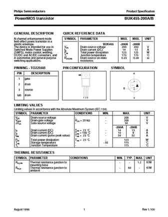
Philips Semiconductors Product Specification PowerMOS transistor BUK455-200A/B GENERAL DESCRIPTION QUICK REFERENCE DATA N-channel enhancement mode SYMBOL PARAMETER MAX. MAX. UNIT field-effect power transistor in a plastic envelope. BUK455 -200A -200B The device is intended for use in VDS Drain-source voltage 200 200 V Switched Mode Power Supplies ID Drain current (DC) 14 13 A (SMPS),
9.7. Size:64K philips
buk454-800a-b.pdf 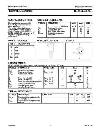
Philips Semiconductors Product Specification PowerMOS transistor BUK454-800A/B GENERAL DESCRIPTION QUICK REFERENCE DATA N-channel enhancement mode SYMBOL PARAMETER MAX. MAX. UNIT field-effect power transistor in a plastic envelope. BUK454 -800A -800B The device is intended for use in VDS Drain-source voltage 800 800 V Switched Mode Power Supplies ID Drain current (DC) 2.4 2.0 A (SMPS)
9.8. Size:56K philips
buk452-100a-b 1.pdf 
Philips Semiconductors Product Specification PowerMOS transistor BUK452-100A/B GENERAL DESCRIPTION QUICK REFERENCE DATA N-channel enhancement mode SYMBOL PARAMETER MAX. MAX. UNIT field-effect power transistor in a plastic envelope. BUK452 -100A -100B The device is intended for use in VDS Drain-source voltage 100 100 V Switched Mode Power Supplies ID Drain current (DC) 11 10 A (SMPS),
9.9. Size:54K philips
buk453-60a-b.pdf 
Philips Semiconductors Product Specification PowerMOS transistor BUK453-60A/B GENERAL DESCRIPTION QUICK REFERENCE DATA N-channel enhancement mode SYMBOL PARAMETER MAX. MAX. UNIT field-effect power transistor in a plastic envelope. BUK453 -60A -60B The device is intended for use in VDS Drain-source voltage 60 60 V Switched Mode Power Supplies ID Drain current (DC) 22 20 A (SMPS), motor
9.10. Size:54K philips
buk455-100a-b 1.pdf 
Philips Semiconductors Product Specification PowerMOS transistor BUK455-100A/B GENERAL DESCRIPTION QUICK REFERENCE DATA N-channel enhancement mode SYMBOL PARAMETER MAX. MAX. UNIT field-effect power transistor in a plastic envelope. BUK455 -100A -100B The device is intended for use in VDS Drain-source voltage 100 100 V Switched Mode Power Supplies ID Drain current (DC) 26 23 A (SMPS),
9.11. Size:50K philips
buk456-200a-b 1.pdf 
Philips Semiconductors Product Specification PowerMOS transistor BUK456-200A/B GENERAL DESCRIPTION QUICK REFERENCE DATA N-channel enhancement mode SYMBOL PARAMETER MAX. MAX. UNIT field-effect power transistor in a plastic envelope. BUK456 -200A -200B The device is intended for use in VDS Drain-source voltage 200 200 V Switched Mode Power Supplies ID Drain current (DC) 19 17 A (SMPS),
9.12. Size:71K philips
buk455-60h 1.pdf 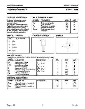
Philips Semiconductors Product specification PowerMOS transistor BUK455-60H GENERAL DESCRIPTION QUICK REFERENCE DATA N-channel enhancement mode SYMBOL PARAMETER MAX. UNIT field-effect power transistor in a plastic envelope. VDS Drain-source voltage 60 V The device is intended for use in ID Drain current (DC) 43 A Automotive applications, Switched Ptot Total power dissipation 125 W Mod
9.13. Size:51K philips
buk454-60h 1.pdf 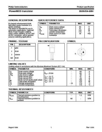
Philips Semiconductors Product specification PowerMOS transistor BUK454-60H GENERAL DESCRIPTION QUICK REFERENCE DATA N-channel enhancement mode SYMBOL PARAMETER MAX. UNIT field-effect power transistor in a plastic envelope. VDS Drain-source voltage 60 V The device is intended for use in ID Drain current (DC) 41 A automotive applications, Switched Ptot Total power dissipation 125 W Mod
9.14. Size:49K philips
buk456-800a-b.pdf 
Philips Semiconductors Product Specification PowerMOS transistor BUK456-800A/B GENERAL DESCRIPTION QUICK REFERENCE DATA N-channel enhancement mode SYMBOL PARAMETER MAX. MAX. UNIT field-effect power transistor in a plastic envelope. BUK456 -800A -800B The device is intended for use in VDS Drain-source voltage 800 800 V Switched Mode Power Supplies ID Drain current (DC) 4 3.5 A (SMPS),
9.15. Size:58K philips
buk454-200a-b 1.pdf 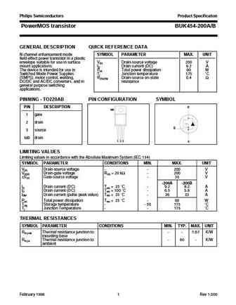
Philips Semiconductors Product Specification PowerMOS transistor BUK454-200A/B GENERAL DESCRIPTION QUICK REFERENCE DATA N-channel enhancement mode SYMBOL PARAMETER MAX. UNIT field-effect power transistor in a plastic envelope suitable for use in surface VDS Drain-source voltage 200 V mount applications. ID Drain current (DC) 9.2 A The device is intended for use in Ptot Total power diss
9.16. Size:48K philips
buk451-100a-b 1.pdf 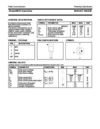
Philips Semiconductors Preliminary Specification PowerMOS transistor BUK451-100A/B GENERAL DESCRIPTION QUICK REFERENCE DATA N-channel enhancement mode SYMBOL PARAMETER MAX. MAX. UNIT field-effect power transistor in a plastic envelope. BUK451 -100A -100B The device is intended for use in VDS Drain-source voltage 100 100 V Switched Mode Power Supplies ID Drain current (DC) 3.0 3.0 A (S
9.17. Size:67K philips
buk456-60a-b 2.pdf 
Philips Semiconductors Product Specification PowerMOS transistor BUK456-60A/B GENERAL DESCRIPTION QUICK REFERENCE DATA N-channel enhancement mode SYMBOL PARAMETER MAX. MAX. UNIT field-effect power transistor in a plastic envelope. BUK456 -60A -60B The device is intended for use in VDS Drain-source voltage 60 60 V Switched Mode Power Supplies ID Drain current (DC) 52 51 A (SMPS), motor
9.18. Size:53K philips
buk455-200b.pdf 
Philips Semiconductors Product Specification PowerMOS transistor BUK455-200A/B GENERAL DESCRIPTION QUICK REFERENCE DATA N-channel enhancement mode SYMBOL PARAMETER MAX. MAX. UNIT field-effect power transistor in a plastic envelope. BUK455 -200A -200B The device is intended for use in VDS Drain-source voltage 200 200 V Switched Mode Power Supplies ID Drain current (DC) 14 13 A (SMPS),
9.19. Size:79K philips
buk455.pdf 
Philips Semiconductors Product Specification PowerMOS transistor BUK455-60A/B GENERAL DESCRIPTION QUICK REFERENCE DATA N-channel enhancement mode SYMBOL PARAMETER MAX. MAX. UNIT field-effect power transistor in a plastic envelope. BUK455 -60A -60B The device is intended for use in VDS Drain-source voltage 60 60 V Switched Mode Power Supplies ID Drain current (DC) 41 38 A (SMPS), motor
9.20. Size:57K philips
buk456-60h 1.pdf 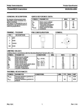
Philips Semiconductors Product Specification PowerMOS transistor BUK456-60H GENERAL DESCRIPTION QUICK REFERENCE DATA N-channel enhancement mode SYMBOL PARAMETER MAX. UNIT field-effect power transistor in a plastic envelope. VDS Drain-source voltage 60 V The device is intended for use in ID Drain current (DC) 60 A Automotive and general purpose Ptot Total power dissipation 150 W switch
9.21. Size:61K philips
buk452-100b.pdf 
Philips Semiconductors Product Specification PowerMOS transistor BUK452-100A/B GENERAL DESCRIPTION QUICK REFERENCE DATA N-channel enhancement mode SYMBOL PARAMETER MAX. MAX. UNIT field-effect power transistor in a plastic envelope. BUK452 -100A -100B The device is intended for use in VDS Drain-source voltage 100 100 V Switched Mode Power Supplies ID Drain current (DC) 11 10 A (SMPS),
9.22. Size:56K philips
buk455-60a-b 1.pdf 
Philips Semiconductors Product Specification PowerMOS transistor BUK455-60A/B GENERAL DESCRIPTION QUICK REFERENCE DATA N-channel enhancement mode SYMBOL PARAMETER MAX. MAX. UNIT field-effect power transistor in a plastic envelope. BUK455 -60A -60B The device is intended for use in VDS Drain-source voltage 60 60 V Switched Mode Power Supplies ID Drain current (DC) 41 38 A (SMPS), motor
9.23. Size:54K philips
buk452-60a-b 1.pdf 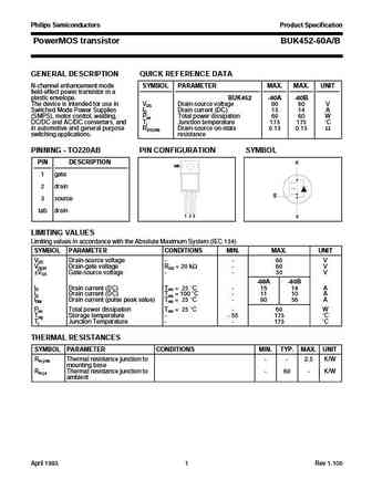
Philips Semiconductors Product Specification PowerMOS transistor BUK452-60A/B GENERAL DESCRIPTION QUICK REFERENCE DATA N-channel enhancement mode SYMBOL PARAMETER MAX. MAX. UNIT field-effect power transistor in a plastic envelope. BUK452 -60A -60B The device is intended for use in VDS Drain-source voltage 60 60 V Switched Mode Power Supplies ID Drain current (DC) 15 14 A (SMPS), motor
9.24. Size:54K philips
buk453-60a-b 1.pdf 
Philips Semiconductors Product Specification PowerMOS transistor BUK453-60A/B GENERAL DESCRIPTION QUICK REFERENCE DATA N-channel enhancement mode SYMBOL PARAMETER MAX. MAX. UNIT field-effect power transistor in a plastic envelope. BUK453 -60A -60B The device is intended for use in VDS Drain-source voltage 60 60 V Switched Mode Power Supplies ID Drain current (DC) 22 20 A (SMPS), motor
9.25. Size:56K philips
buk455-60a-b.pdf 
Philips Semiconductors Product Specification PowerMOS transistor BUK455-60A/B GENERAL DESCRIPTION QUICK REFERENCE DATA N-channel enhancement mode SYMBOL PARAMETER MAX. MAX. UNIT field-effect power transistor in a plastic envelope. BUK455 -60A -60B The device is intended for use in VDS Drain-source voltage 60 60 V Switched Mode Power Supplies ID Drain current (DC) 41 38 A (SMPS), motor
9.26. Size:48K philips
buk455-100b.pdf 
Philips Semiconductors Product Specification PowerMOS transistor BUK455-100A/B GENERAL DESCRIPTION QUICK REFERENCE DATA N-channel enhancement mode SYMBOL PARAMETER MAX. MAX. UNIT field-effect power transistor in a plastic envelope. BUK455 -100A -100B The device is intended for use in VDS Drain-source voltage 100 100 V Switched Mode Power Supplies ID Drain current (DC) 26 23 A (SMPS),
9.27. Size:228K inchange semiconductor
buk456-100.pdf 
isc N-Channel MOSFET Transistor BUK456-100A/B DESCRIPTION Drain Source Voltage- V =100V(Min) DSS Low R DS(ON) Fast Switching Speed Minimum Lot-to-Lot variations for robust device performance and reliable operation APPLICATIONS Designed for Switched Mode Power Supplies (SMPS), motor control,welding, and in general purpose switching resistance application ABSOLUTE MAXIMU
9.28. Size:229K inchange semiconductor
buk455-60.pdf 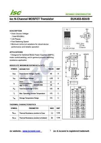
isc N-Channel MOSFET Transistor BUK455-60A/B DESCRIPTION Drain Source Voltage- V =60V(Min) DSS Low R DS(ON) Fast Switching Speed Minimum Lot-to-Lot variations for robust device performance and reliable operation APPLICATIONS Designed for Switched Mode Power Supplies (SMPS), motor control,welding, and in general purpose switching resistance application ABSOLUTE MAXIMUM
9.29. Size:229K inchange semiconductor
buk456-200.pdf 
isc N-Channel MOSFET Transistor BUK456-200A/B DESCRIPTION Drain Source Voltage- V =200V(Min) DSS Low R DS(ON) Fast Switching Speed Minimum Lot-to-Lot variations for robust device performance and reliable operation APPLICATIONS Designed for Switched Mode Power Supplies (SMPS), motor control,welding, and in general purpose switching resistance application ABSOLUTE MAXIMU
9.30. Size:228K inchange semiconductor
buk455-200.pdf 
isc N-Channel MOSFET Transistor BUK455-200A/B DESCRIPTION Drain Source Voltage- V =200V(Min) DSS Low R DS(ON) Fast Switching Speed Minimum Lot-to-Lot variations for robust device performance and reliable operation APPLICATIONS Designed for Switched Mode Power Supplies (SMPS), motor control,welding, and in general purpose switching resistance application ABSOLUTE MAXIMU
9.31. Size:228K inchange semiconductor
buk452-60.pdf 
isc N-Channel MOSFET Transistor BUK452-60A/B DESCRIPTION Drain Source Voltage- V =60V(Min) DSS Low R DS(ON) Fast Switching Speed Minimum Lot-to-Lot variations for robust device performance and reliable operation APPLICATIONS Designed for Switched Mode Power Supplies (SMPS), motor control,welding, and in general purpose switching resistance application ABSOLUTE MAXIMUM
9.32. Size:228K inchange semiconductor
buk452-100.pdf 
isc N-Channel MOSFET Transistor BUK452-100A/B DESCRIPTION Drain Source Voltage- V =100V(Min) DSS Low R DS(ON) Fast Switching Speed Minimum Lot-to-Lot variations for robust device performance and reliable operation APPLICATIONS Designed for Switched Mode Power Supplies (SMPS), motor control,welding, and in general purpose switching resistance application ABSOLUTE MAXIMU
9.33. Size:228K inchange semiconductor
buk455-100.pdf 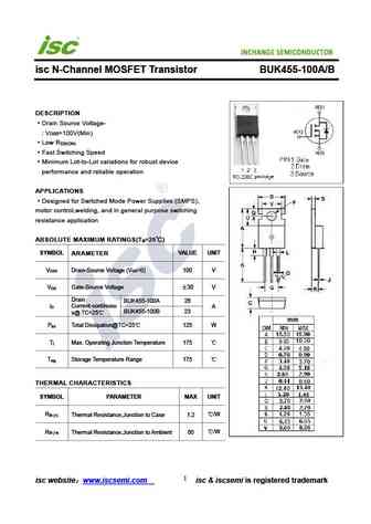
isc N-Channel MOSFET Transistor BUK455-100A/B DESCRIPTION Drain Source Voltage- V =100V(Min) DSS Low R DS(ON) Fast Switching Speed Minimum Lot-to-Lot variations for robust device performance and reliable operation APPLICATIONS Designed for Switched Mode Power Supplies (SMPS), motor control,welding, and in general purpose switching resistance application ABSOLUTE MAXIMU
9.34. Size:229K inchange semiconductor
buk453-60.pdf 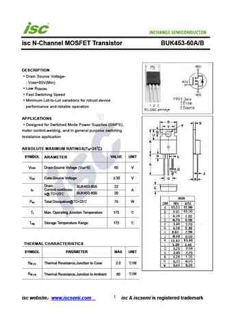
isc N-Channel MOSFET Transistor BUK453-60A/B DESCRIPTION Drain Source Voltage- V =60V(Min) DSS Low R DS(ON) Fast Switching Speed Minimum Lot-to-Lot variations for robust device performance and reliable operation APPLICATIONS Designed for Switched Mode Power Supplies (SMPS), motor control,welding, and in general purpose switching resistance application ABSOLUTE MAXIMUM
9.35. Size:229K inchange semiconductor
buk456-800.pdf 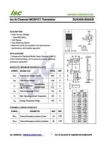
isc N-Channel MOSFET Transistor BUK456-800A/B DESCRIPTION Drain Source Voltage- V =800V(Min) DSS Low R DS(ON) Fast Switching Speed Minimum Lot-to-Lot variations for robust device performance and reliable operation APPLICATIONS Designed for Switched Mode Power Supplies (SMPS), motor control,welding, and in general purpose switching resistance application ABSOLUTE MAXIMU
9.36. Size:229K inchange semiconductor
buk454-800.pdf 
isc N-Channel MOSFET Transistor BUK454-800A/B DESCRIPTION Drain Source Voltage- V =800V(Min) DSS Low R DS(ON) Fast Switching Speed Minimum Lot-to-Lot variations for robust device performance and reliable operation APPLICATIONS Designed for Switched Mode Power Supplies (SMPS), motor control,welding, and in general purpose switching resistance application ABSOLUTE MAXIMU
9.37. Size:228K inchange semiconductor
buk454-200.pdf 
isc N-Channel MOSFET Transistor BUK454-200A/B DESCRIPTION Drain Source Voltage- V =200V(Min) DSS Low R DS(ON) Fast Switching Speed Minimum Lot-to-Lot variations for robust device performance and reliable operation APPLICATIONS Designed for Switched Mode Power Supplies (SMPS), motor control,welding, and in general purpose switching resistance application ABSOLUTE MAXIMU
9.38. Size:228K inchange semiconductor
buk453-100.pdf 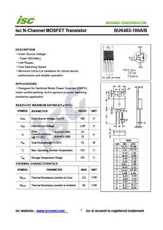
isc N-Channel MOSFET Transistor BUK453-100A/B DESCRIPTION Drain Source Voltage- V =100V(Min) DSS Low R DS(ON) Fast Switching Speed Minimum Lot-to-Lot variations for robust device performance and reliable operation APPLICATIONS Designed for Switched Mode Power Supplies (SMPS), motor control,welding, and in general purpose switching resistance application ABSOLUTE MAXIMU
9.39. Size:229K inchange semiconductor
buk456-60.pdf 
isc N-Channel MOSFET Transistor BUK456-60A/B DESCRIPTION Drain Source Voltage- V =60V(Min) DSS Low R DS(ON) Fast Switching Speed Minimum Lot-to-Lot variations for robust device performance and reliable operation APPLICATIONS Designed for Switched Mode Power Supplies (SMPS), motor control,welding, and in general purpose switching resistance application ABSOLUTE MAXIMUM
Другие MOSFET... APT5014BFLLG
, APT5014BLLG
, APT5014LVFRG
, APT5014SFLLG
, APT5014SLLG
, APT5015BVFRG
, 2SK1982-01MR
, BUK457-400A
, IRFZ24N
, 2SK125
, 2SJ410
, 2SK2518-01MR
, 2SK4027
, APT5016BFLLG
, APT5016BLLG
, APT5016SFLLG
, APT5017SVFRG
.
History: SID9971
| AP3N2R8H
| SES760
| HY1001P
| BUK457-400A
| 2SJ0582
| NCE60R360