APT6033BN Datasheet. Specs and Replacement
Type Designator: APT6033BN 📄📄
Type of Transistor: MOFETS
Type of Control Channel: N-Channel
Absolute Maximum Ratings
Pd ⓘ - Maximum Power Dissipation: 360 W
|Vds|ⓘ - Maximum Drain-Source Voltage: 600 V
|Vgs|ⓘ - Maximum Gate-Source Voltage: 30 V
|Id| ⓘ - Maximum Drain Current: 22 A
Tj ⓘ - Maximum Junction Temperature: 150 °C
Electrical Characteristics
tr ⓘ - Rise Time: 35 nS
Cossⓘ - Output Capacitance: 505 pF
RDSonⓘ - Maximum Drain-Source On-State Resistance: 0.33 Ohm
Package: TO-247
📄📄 Copy
- MOSFET ⓘ Cross-Reference Search
APT6033BN datasheet
..1. Size:47K apt
apt6033bn.pdf 
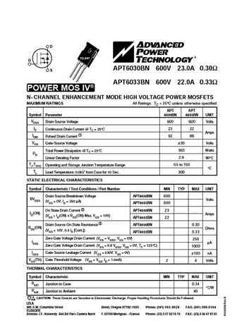
D TO-247 G APT6030BN 600V 23.0A 0.30 S APT6033BN 600V 22.0A 0.33 POWER MOS IV N- CHANNEL ENHANCEMENT MODE HIGH VOLTAGE POWER MOSFETS MAXIMUM RATINGS All Ratings TC = 25 C unless otherwise specified. APT APT Symbol Parameter 6030BN 6033BN UNIT VDSS Drain-Source Voltage 600 600 Volts ID Continuous Drain Current @ TC = 25 C 23 22 Amps IDM Pulsed Drain Current 1 92 88 V... See More ⇒
8.1. Size:61K apt
apt6030bvr.pdf
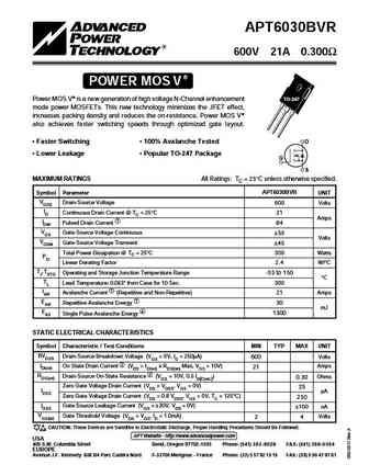
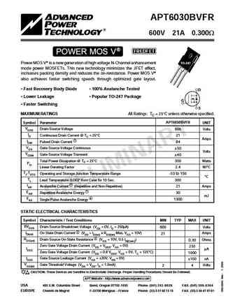
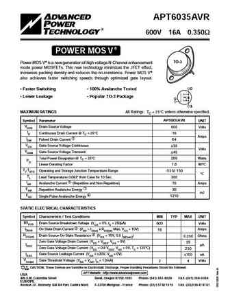
APT6030BVR 600V 21A 0.300 POWER MOS V Power MOS V is a new generation of high voltage N-Channel enhancement TO-247 mode power MOSFETs. This new technology minimizes the JFET effect, increases packing density and reduces the on-resistance. Power MOS V also achieves faster switching speeds through optimized gate layout. Faster Switching 100% Avalanche Tested D Lower L... See More ⇒
8.2. Size:49K apt
apt6035bn.pdf
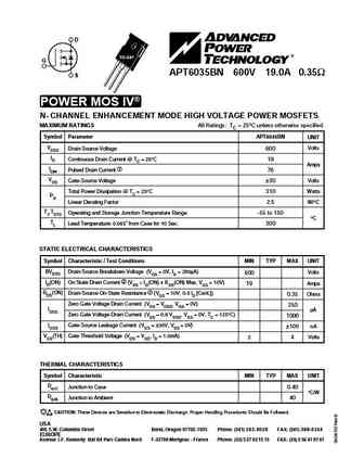
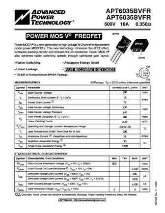
D TO-247 G APT6035BN 600V 19.0A 0.35 S POWER MOS IV N- CHANNEL ENHANCEMENT MODE HIGH VOLTAGE POWER MOSFETS MAXIMUM RATINGS All Ratings TC = 25 C unless otherwise specified. Symbol Parameter APT6035BN UNIT VDSS Drain-Source Voltage 600 Volts ID Continuous Drain Current @ TC = 25 C 19 Amps IDM Pulsed Drain Current 1 76 VGS Gate-Source Voltage 30 Volts Total Power Dissi... See More ⇒
8.3. Size:62K apt
apt6035bvr.pdf

APT6035BVR 600V 18A 0.350 POWER MOS V Power MOS V is a new generation of high voltage N-Channel enhancement TO-247 mode power MOSFETs. This new technology minimizes the JFET effect, increases packing density and reduces the on-resistance. Power MOS V also achieves faster switching speeds through optimized gate layout. Faster Switching 100% Avalanche Tested D Lower L... See More ⇒
8.4. Size:62K apt
apt6035.pdf

APT6035AVR 600V 16A 0.350 POWER MOS V TO-3 Power MOS V is a new generation of high voltage N-Channel enhancement mode power MOSFETs. This new technology minimizes the JFET effect, increases packing density and reduces the on-resistance. Power MOS V also achieves faster switching speeds through optimized gate layout. D Faster Switching 100% Avalanche Tested Lower L... See More ⇒
8.5. Size:136K apt
apt6030svfr.pdf

APT6030BVFR APT6030SVFR 600V 21A 0.300 BVFR POWER MOS V FREDFET D3PAK Power MOS V is a new generation of high voltage N-Channel enhancement TO-247 mode power MOSFETs. This new technology minimizes the JFET effect, increases packing density and reduces the on-resistance. Power MOS V also achieves faster switching speeds through optimized gate layout. SVFR... See More ⇒
8.6. Size:61K apt
apt6037hvr.pdf

APT6037HVR 600V 15.5A 0.370 POWER MOS V TO-258 Power MOS V is a new generation of high voltage N-Channel enhancement mode power MOSFETs. This new technology minimizes the JFET effect, increases packing density and reduces the on-resistance. Power MOS V also achieves faster switching speeds through optimized gate layout. Faster Switching 100% Avalanche Tested D Lowe... See More ⇒
8.7. Size:61K apt
apt6032avr.pdf
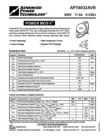
APT6032AVR 600V 17.5A 0.320 POWER MOS V TO-3 Power MOS V is a new generation of high voltage N-Channel enhancement mode power MOSFETs. This new technology minimizes the JFET effect, increases packing density and reduces the on-resistance. Power MOS V also achieves faster switching speeds through optimized gate layout. D Faster Switching 100% Avalanche Tested Lower... See More ⇒
8.8. Size:62K apt
apt6030bvfr.pdf
APT6030BVFR 600V 21A 0.300W POWER MOS V FREDFET Power MOS V is a new generation of high voltage N-Channel enhancement TO-247 mode power MOSFETs. This new technology minimizes the JFET effect, increases packing density and reduces the on-resistance. Power MOS V also achieves faster switching speeds through optimized gate layout. Fast Recovery Body Diode 100% Avalanche Tested... See More ⇒
8.9. Size:71K apt
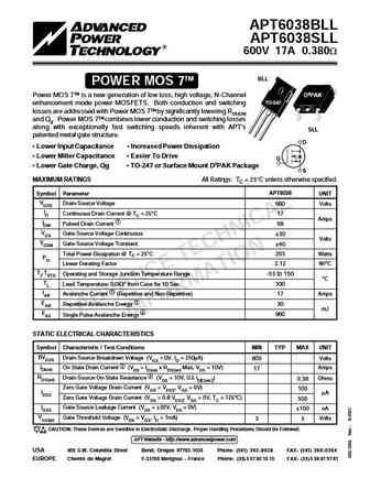
apt6038bfll.pdf
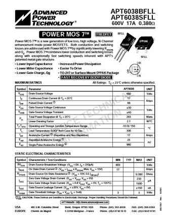
APT6038BFLL APT6038SFLL 600V 17A 0.380W TM BFLL FREDFET POWER MOS 7 Power MOS 7TM is a new generation of low loss, high voltage, N-Channel D3PAK TO-247 enhancement mode power MOSFETS. Both conduction and switching losses are addressed with Power MOS 7TM by significantly lowering RDS(ON) and Qg. Power MOS 7TM combines lower conduction and switching losses along with exceptionally fas... See More ⇒
8.10. Size:112K apt
apt6030svr.pdf
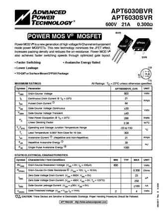
APT6030BVR APT6030SVR 600V 21A 0.300 BVR POWER MOS V MOSFET D3PAK Power MOS V is a new generation of high voltage N-Channel enhancement TO-247 mode power MOSFETs. This new technology minimizes the JFET effect, increases packing density and reduces the on-resistance. Power MOS V also achieves faster switching speeds through optimized gate layout. SVR ... See More ⇒
8.11. Size:117K apt
apt6035bvfrg apt6035svfrg.pdf
APT6035BVFR APT6035SVFR 600V 18A 0.350 BVFR POWER MOS V FREDFET D3PAK Power MOS V is a new generation of high voltage N-Channel enhancement TO-247 mode power MOSFETs. This new technology minimizes the JFET effect, increases packing density and reduces the on-resistance. Power MOS V also achieves faster switching speeds through optimized gate layout. SVFR... See More ⇒
8.12. Size:69K apt
apt6038bll.pdf
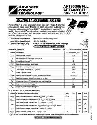
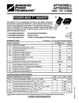
APT6038BLL APT6038SLL 600V 17A 0.380W TM BLL POWER MOS 7 Power MOS 7TM is a new generation of low loss, high voltage, N-Channel D3PAK TO-247 enhancement mode power MOSFETS. Both conduction and switching losses are addressed with Power MOS 7TM by significantly lowering RDS(ON) and Qg. Power MOS 7TM combines lower conduction and switching losses along with exceptionally fast switching ... See More ⇒
8.13. Size:162K apt
apt6038bfllg apt6038sfllg.pdf
APT6038BFLL APT6038SFLL 600V 17A 0.380 R BFLL POWER MOS 7 FREDFET D3PAK Power MOS 7 is a new generation of low loss, high voltage, N-Channel TO-247 enhancement mode power MOSFETS. Both conduction and switching losses are addressed with Power MOS 7 by significantly lowering RDS(ON) and Qg. Power MOS 7 combines lower conduction and switching losses SFLL a... See More ⇒
8.14. Size:161K apt
apt6038bllg apt6038sllg.pdf
APT6038BLL APT6038SLL 600V 17A 0.380 R BLL POWER MOS 7 MOSFET D3PAK TO-247 Power MOS 7 is a new generation of low loss, high voltage, N-Channel enhancement mode power MOSFETS. Both conduction and switching losses are addressed with Power MOS 7 by significantly lowering RDS(ON) and Qg. Power MOS 7 combines lower conduction and switching losses SLL along... See More ⇒
8.15. Size:116K apt
apt6035bvfr.pdf

APT6035BVFR APT6035SVFR 600V 18A 0.350 BVFR POWER MOS V FREDFET D3PAK Power MOS V is a new generation of high voltage N-Channel enhancement TO-247 mode power MOSFETs. This new technology minimizes the JFET effect, increases packing density and reduces the on-resistance. Power MOS V also achieves faster switching speeds through optimized gate layout. SVFR... See More ⇒
8.16. Size:65K apt
apt6035svr.pdf
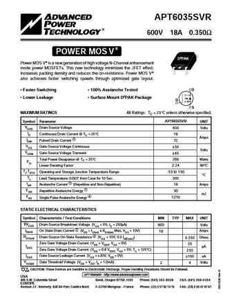
APT6035SVR 600V 18A 0.350 POWER MOS V D3PAK Power MOS V is a new generation of high voltage N-Channel enhancement mode power MOSFETs. This new technology minimizes the JFET effect, increases packing density and reduces the on-resistance. Power MOS V also achieves faster switching speeds through optimized gate layout. D Faster Switching 100% Avalanche Tested Lower ... See More ⇒
8.17. Size:51K apt
apt6030bn.pdf
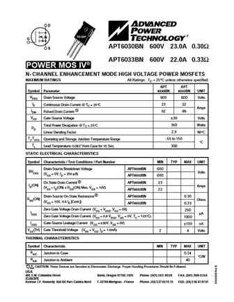
D TO-247 G APT6030BN 600V 23.0A 0.30 S APT6033BN 600V 22.0A 0.33 POWER MOS IV N- CHANNEL ENHANCEMENT MODE HIGH VOLTAGE POWER MOSFETS MAXIMUM RATINGS All Ratings TC = 25 C unless otherwise specified. APT APT Symbol Parameter 6030BN 6033BN UNIT VDSS Drain-Source Voltage 600 600 Volts ID Continuous Drain Current @ TC = 25 C 23 22 Amps IDM Pulsed Drain Current 1 92 88 V... See More ⇒
8.18. Size:62K apt
apt6030.pdf

APT6030BVFR 600V 21A 0.300W POWER MOS V FREDFET Power MOS V is a new generation of high voltage N-Channel enhancement TO-247 mode power MOSFETs. This new technology minimizes the JFET effect, increases packing density and reduces the on-resistance. Power MOS V also achieves faster switching speeds through optimized gate layout. Fast Recovery Body Diode 100% Avalanche Tested... See More ⇒
8.19. Size:62K apt
apt6035avr.pdf
APT6035AVR 600V 16A 0.350 POWER MOS V TO-3 Power MOS V is a new generation of high voltage N-Channel enhancement mode power MOSFETs. This new technology minimizes the JFET effect, increases packing density and reduces the on-resistance. Power MOS V also achieves faster switching speeds through optimized gate layout. D Faster Switching 100% Avalanche Tested Lower L... See More ⇒
8.20. Size:376K inchange semiconductor
apt6030bvr.pdf

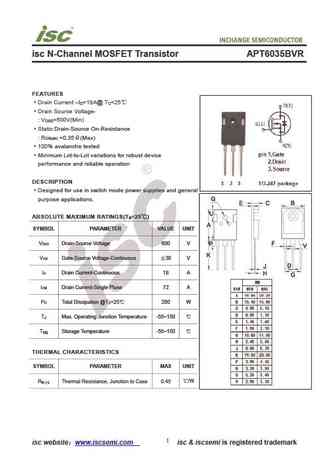
isc N-Channel MOSFET Transistor APT6030BVR FEATURES Drain Current I =21A@ T =25 D C Drain Source Voltage- V =600V(Min) DSS Static Drain-Source On-Resistance R =0.3 (Max) DS(on) 100% avalanche tested Minimum Lot-to-Lot variations for robust device performance and reliable operation DESCRIPTION Designed for use in switch mode power supplies and general purpos... See More ⇒
8.21. Size:376K inchange semiconductor
apt6035bvr.pdf
isc N-Channel MOSFET Transistor APT6035BVR FEATURES Drain Current I =18A@ T =25 D C Drain Source Voltage- V =600V(Min) DSS Static Drain-Source On-Resistance R =0.35 (Max) DS(on) 100% avalanche tested Minimum Lot-to-Lot variations for robust device performance and reliable operation DESCRIPTION Designed for use in switch mode power supplies and general purpo... See More ⇒
8.22. Size:376K inchange semiconductor
apt6030bvfr.pdf

isc N-Channel MOSFET Transistor APT6030BVFR FEATURES Drain Current I =21A@ T =25 D C Drain Source Voltage- V =600V(Min) DSS Static Drain-Source On-Resistance R =0.3 (Max) DS(on) 100% avalanche tested Minimum Lot-to-Lot variations for robust device performance and reliable operation DESCRIPTION Designed for use in switch mode power supplies and general purpo... See More ⇒
8.23. Size:376K inchange semiconductor
apt6038bfll.pdf
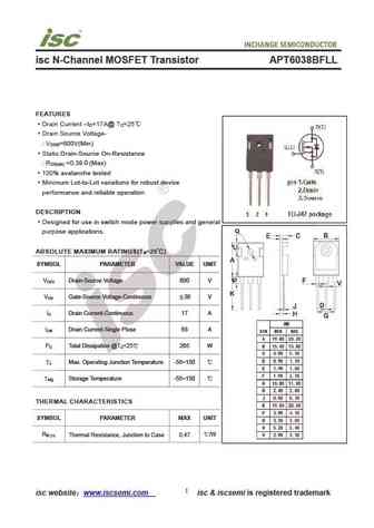
isc N-Channel MOSFET Transistor APT6038BFLL FEATURES Drain Current I =17A@ T =25 D C Drain Source Voltage- V =600V(Min) DSS Static Drain-Source On-Resistance R =0.38 (Max) DS(on) 100% avalanche tested Minimum Lot-to-Lot variations for robust device performance and reliable operation DESCRIPTION Designed for use in switch mode power supplies and general purp... See More ⇒
8.24. Size:376K inchange semiconductor
apt6038bll.pdf

isc N-Channel MOSFET Transistor APT6038BLL FEATURES Drain Current I =17A@ T =25 D C Drain Source Voltage- V =600V(Min) DSS Static Drain-Source On-Resistance R =0.38 (Max) DS(on) 100% avalanche tested Minimum Lot-to-Lot variations for robust device performance and reliable operation DESCRIPTION Designed for use in switch mode power supplies and general purpo... See More ⇒
Detailed specifications: APT6025BVFRG, APT6025BVRG, APT6025SFLLG, APT6025SVFRG, APT6029BFLLG, APT6029SFLLG, APT6029SLL, APT6029SLLG, IRF1405, APT6035BVFRG, APT6035SVFRG, APT6038BFLLG, APT6038BLLG, APT6038SFLLG, APT6038SLLG, APT6040SVFR, APT6040SVR
Keywords - APT6033BN MOSFET specs
APT6033BN cross reference
APT6033BN equivalent finder
APT6033BN pdf lookup
APT6033BN substitution
APT6033BN replacement
Need a MOSFET replacement?
Our guide shows you how to find a perfect substitute by comparing key parameters and specs
