NTD4910N-1G Specs and Replacement
Type Designator: NTD4910N-1G
Type of Transistor: MOSFET
Type of Control Channel: N-Channel
Absolute Maximum Ratings
Pd ⓘ
- Maximum Power Dissipation: 27.3 W
|Vds|ⓘ - Maximum Drain-Source Voltage: 30 V
|Vgs|ⓘ - Maximum Gate-Source Voltage: 20 V
|Id| ⓘ - Maximum Drain Current: 37 A
Tj ⓘ - Maximum Junction Temperature: 175 °C
Electrical Characteristics
tr ⓘ - Rise Time: 21.8 nS
Cossⓘ -
Output Capacitance: 460 pF
RDSonⓘ - Maximum Drain-Source On-State Resistance: 0.009 Ohm
Package: DPAK
IPAK
- MOSFET ⓘ Cross-Reference Search
NTD4910N-1G datasheet
..1. Size:138K onsemi
ntd4910n-1g.pdf 

NTD4910N Power MOSFET 30 V, 37 A, Single N-Channel, DPAK/IPAK Features Low RDS(on) to Minimize Conduction Losses Low Capacitance to Minimize Driver Losses http //onsemi.com Optimized Gate Charge to Minimize Switching Losses These are Pb-Free Devices V(BR)DSS RDS(on) MAX ID MAX Applications 9.0 mW @ 10 V CPU Power Delivery 30 V 37 A 13 mW @ 4.5 V DC-DC Conv... See More ⇒
6.1. Size:108K onsemi
ntd4910n.pdf
NTD4910N Power MOSFET 30 V, 37 A, Single N-Channel, DPAK/IPAK Features Low RDS(on) to Minimize Conduction Losses Low Capacitance to Minimize Driver Losses http //onsemi.com Optimized Gate Charge to Minimize Switching Losses These are Pb-Free Devices V(BR)DSS RDS(on) MAX ID MAX Applications 9.0 mW @ 10 V CPU Power Delivery 30 V 37 A 13 mW @ 4.5 V DC-DC Conv... See More ⇒
8.1. Size:140K onsemi
ntd4913n.pdf
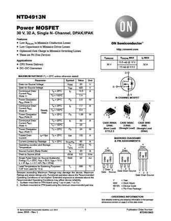
NTD4913N Power MOSFET 30 V, 32 A, Single N-Channel, DPAK/IPAK Features Low RDS(on) to Minimize Conduction Losses Low Capacitance to Minimize Driver Losses http //onsemi.com Optimized Gate Charge to Minimize Switching Losses These are Pb-Free Devices V(BR)DSS RDS(ON) MAX ID MAX Applications 10.5 mW @ 10 V CPU Power Delivery 30 V 32 A 15 mW @ 4.5 V DC-DC Con... See More ⇒
9.1. Size:123K 1
ntd4963ng.pdf
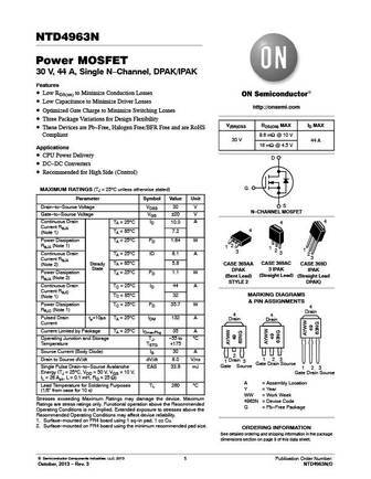
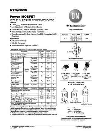
NTD4963N Power MOSFET 30 V, 44 A, Single N-Channel, DPAK/IPAK Features Low RDS(on) to Minimize Conduction Losses Low Capacitance to Minimize Driver Losses http //onsemi.com Optimized Gate Charge to Minimize Switching Losses Three Package Variations for Design Flexibility V(BR)DSS RDS(ON) MAX ID MAX These Devices are Pb-Free, Halogen Free/BFR Free and are RoHS 9.6 ... See More ⇒
9.3. Size:86K onsemi
ntd4904n.pdf
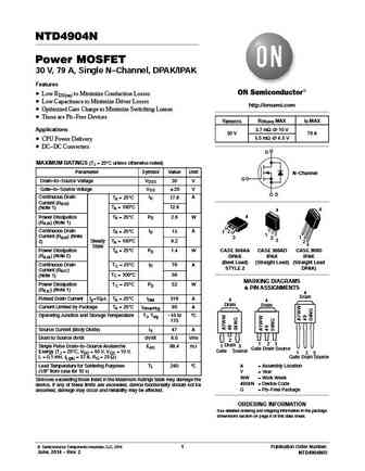
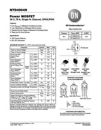
NTD4904N Power MOSFET 30 V, 79 A, Single N-Channel, DPAK/IPAK Features Low RDS(on) to Minimize Conduction Losses Low Capacitance to Minimize Driver Losses http //onsemi.com Optimized Gate Charge to Minimize Switching Losses These are Pb-Free Devices V(BR)DSS RDS(on) MAX ID MAX Applications 3.7 mW @ 10 V 30 V 79 A 5.5 mW @ 4.5 V CPU Power Delivery DC-DC Conv... See More ⇒
9.4. Size:140K onsemi
ntd4970n.pdf
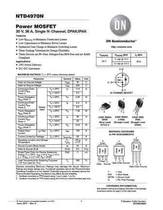
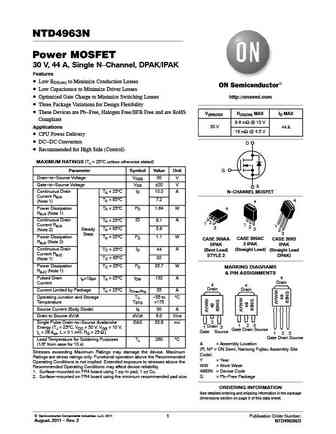
NTD4970N Power MOSFET 30 V, 36 A, Single N-Channel, DPAK/IPAK Features Low RDS(on) to Minimize Conduction Losses Low Capacitance to Minimize Driver Losses Optimized Gate Charge to Minimize Switching Losses http //onsemi.com Three Package Variations for Design Flexibility These Devices are Pb-Free, Halogen Free/BFR Free and are RoHS V(BR)DSS RDS(ON) MAX ID MAX Compl... See More ⇒
9.5. Size:123K onsemi
ntd4906n.pdf
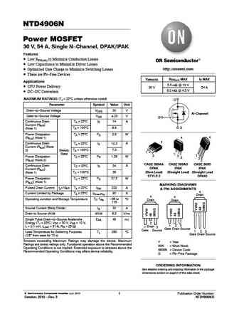
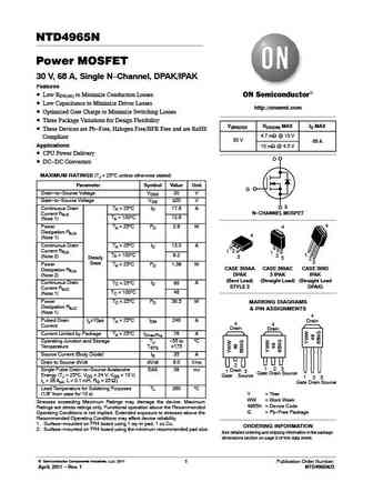
NTD4906N Power MOSFET 30 V, 54 A, Single N-Channel, DPAK/IPAK Features Low RDS(on) to Minimize Conduction Losses Low Capacitance to Minimize Driver Losses http //onsemi.com Optimized Gate Charge to Minimize Switching Losses These are Pb-Free Devices V(BR)DSS RDS(on) MAX ID MAX Applications 5.5 mW @ 10 V CPU Power Delivery 30 V 54 A 8.0 mW @ 4.5 V DC-DC Con... See More ⇒
9.6. Size:118K onsemi
ntd4969n-d.pdf

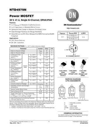
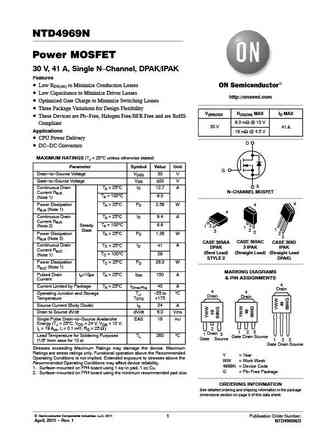
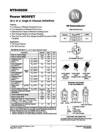
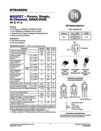
NTD4969N Power MOSFET 30 V, 41 A, Single N-Channel, DPAK/IPAK Features Low RDS(on) to Minimize Conduction Losses Low Capacitance to Minimize Driver Losses http //onsemi.com Optimized Gate Charge to Minimize Switching Losses Three Package Variations for Design Flexibility V(BR)DSS RDS(ON) MAX ID MAX These Devices are Pb-Free, Halogen Free/BFR Free and are RoHS 9.0 ... See More ⇒
9.7. Size:114K onsemi
ntd4969n-1g.pdf
NTD4969N Power MOSFET 30 V, 41 A, Single N-Channel, DPAK/IPAK Features Low RDS(on) to Minimize Conduction Losses Low Capacitance to Minimize Driver Losses http //onsemi.com Optimized Gate Charge to Minimize Switching Losses Three Package Variations for Design Flexibility V(BR)DSS RDS(ON) MAX ID MAX These Devices are Pb-Free, Halogen Free/BFR Free and are RoHS 9.0 ... See More ⇒
9.8. Size:82K onsemi
ntd4969n.pdf
NTD4969N Power MOSFET 30 V, 41 A, Single N-Channel, DPAK/IPAK Features Low RDS(on) to Minimize Conduction Losses Low Capacitance to Minimize Driver Losses http //onsemi.com Optimized Gate Charge to Minimize Switching Losses Three Package Variations for Design Flexibility V(BR)DSS RDS(ON) MAX ID MAX These Devices are Pb-Free, Halogen Free/BFR Free and are RoHS 9.0 ... See More ⇒
9.9. Size:115K onsemi
ntd4963n-1g.pdf
NTD4963N Power MOSFET 30 V, 44 A, Single N-Channel, DPAK/IPAK Features Low RDS(on) to Minimize Conduction Losses Low Capacitance to Minimize Driver Losses Optimized Gate Charge to Minimize Switching Losses http //onsemi.com Three Package Variations for Design Flexibility These Devices are Pb-Free, Halogen Free/BFR Free and are RoHS V(BR)DSS RDS(ON) MAX ID MAX Compl... See More ⇒
9.10. Size:113K onsemi
ntd4970n-1g.pdf

NTD4970N Power MOSFET 30 V, 36 A, Single N-Channel, DPAK/IPAK Features Low RDS(on) to Minimize Conduction Losses Low Capacitance to Minimize Driver Losses Optimized Gate Charge to Minimize Switching Losses http //onsemi.com Three Package Variations for Design Flexibility These Devices are Pb-Free, Halogen Free/BFR Free and are RoHS V(BR)DSS RDS(ON) MAX ID MAX Compl... See More ⇒
9.11. Size:141K onsemi
ntd4904n-1g ntd4904n.pdf
NTD4904N Power MOSFET 30 V, 79 A, Single N-Channel, DPAK/IPAK Features Low RDS(on) to Minimize Conduction Losses Low Capacitance to Minimize Driver Losses http //onsemi.com Optimized Gate Charge to Minimize Switching Losses These are Pb-Free Devices V(BR)DSS RDS(on) MAX ID MAX Applications 3.7 mW @ 10 V 30 V 79 A 5.5 mW @ 4.5 V CPU Power Delivery DC-DC Conv... See More ⇒
9.12. Size:112K onsemi
ntd4965n-d.pdf
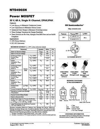
NTD4965N Power MOSFET 30 V, 68 A, Single N-Channel, DPAK/IPAK Features Low RDS(on) to Minimize Conduction Losses Low Capacitance to Minimize Driver Losses http //onsemi.com Optimized Gate Charge to Minimize Switching Losses Three Package Variations for Design Flexibility V(BR)DSS RDS(ON) MAX ID MAX These Devices are Pb-Free, Halogen Free/BFR Free and are RoHS 4.7 ... See More ⇒
9.13. Size:138K onsemi
ntd4960n-1g.pdf
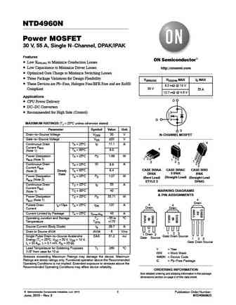
NTD4960N Power MOSFET 30 V, 55 A, Single N-Channel, DPAK/IPAK Features Low RDS(on) to Minimize Conduction Losses Low Capacitance to Minimize Driver Losses http //onsemi.com Optimized Gate Charge to Minimize Switching Losses Three Package Variations for Design Flexibility V(BR)DSS RDS(ON) MAX ID MAX These Devices are Pb-Free, Halogen Free/BFR Free and are RoHS 8.0 ... See More ⇒
9.14. Size:107K onsemi
ntd4965n-1g.pdf
NTD4965N Power MOSFET 30 V, 68 A, Single N-Channel, DPAK/IPAK Features Low RDS(on) to Minimize Conduction Losses Low Capacitance to Minimize Driver Losses http //onsemi.com Optimized Gate Charge to Minimize Switching Losses Three Package Variations for Design Flexibility V(BR)DSS RDS(ON) MAX ID MAX These Devices are Pb-Free, Halogen Free/BFR Free and are RoHS 4.7 ... See More ⇒
9.15. Size:138K onsemi
ntd4909n-1g ntd4909n.pdf
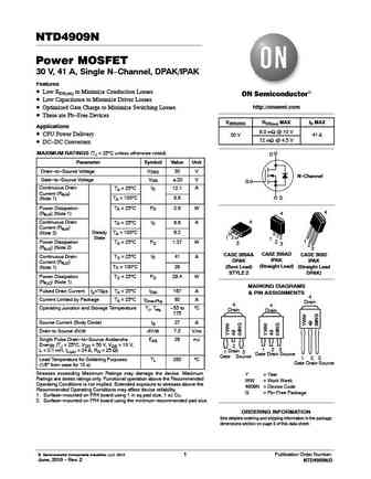
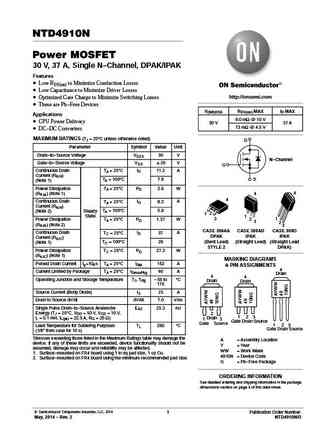
NTD4909N Power MOSFET 30 V, 41 A, Single N-Channel, DPAK/IPAK Features Low RDS(on) to Minimize Conduction Losses Low Capacitance to Minimize Driver Losses http //onsemi.com Optimized Gate Charge to Minimize Switching Losses These are Pb-Free Devices V(BR)DSS RDS(on) MAX ID MAX Applications 8.0 mW @ 10 V CPU Power Delivery 30 V 41 A 12 mW @ 4.5 V DC-DC Conv... See More ⇒
9.16. Size:137K onsemi
ntd4909n.pdf
NTD4909N MOSFET Power, Single, N-Channel, DPAK/IPAK 30 V, 41 A Features Low RDS(on) to Minimize Conduction Losses http //onsemi.com Low Capacitance to Minimize Driver Losses Optimized Gate Charge to Minimize Switching Losses V(BR)DSS RDS(on) MAX ID MAX These are Pb-Free Devices 8.0 mW @ 10 V 30 V 41 A 12 mW @ 4.5 V Applications CPU Power Delivery D DC-... See More ⇒
9.17. Size:139K onsemi
ntd4963n.pdf
NTD4963N Power MOSFET 30 V, 44 A, Single N-Channel, DPAK/IPAK Features Low RDS(on) to Minimize Conduction Losses Low Capacitance to Minimize Driver Losses Optimized Gate Charge to Minimize Switching Losses http //onsemi.com Three Package Variations for Design Flexibility These Devices are Pb-Free, Halogen Free/BFR Free and are RoHS V(BR)DSS RDS(ON) MAX ID MAX Compl... See More ⇒
Detailed specifications: NTD4856N-1G, NTD4857N-1G, NTD4858N-1G, NTD4860N-1G, NTD4863N-1G, NTD4865N-1G, NTD4904N-1G, NTD4909N-1G, RFP50N06, NTD4960N-1G, NTD4963N-1G, NTD4965N-1G, NTD4969N-1G, NTD4970N-1G, NTD50N03R, NTD5406NG, NTD5407NG
Keywords - NTD4910N-1G MOSFET specs
NTD4910N-1G cross reference
NTD4910N-1G equivalent finder
NTD4910N-1G pdf lookup
NTD4910N-1G substitution
NTD4910N-1G replacement
Need a MOSFET replacement?
Our guide shows you how to find a perfect substitute by comparing key parameters and specs