NTLJF4156NTAG Datasheet. Specs and Replacement
Type Designator: NTLJF4156NTAG 📄📄
Type of Transistor: MOSFET
Type of Control Channel: N-Channel
Absolute Maximum Ratings
Pd ⓘ - Maximum Power Dissipation: 0.71 W
|Vds|ⓘ - Maximum Drain-Source Voltage: 30 V
|Vgs|ⓘ - Maximum Gate-Source Voltage: 8 V
|Id| ⓘ - Maximum Drain Current: 2.5 A
Tj ⓘ - Maximum Junction Temperature: 150 °C
Electrical Characteristics
tr ⓘ - Rise Time: 9.2 nS
Cossⓘ - Output Capacitance: 51 pF
RDSonⓘ - Maximum Drain-Source On-State Resistance: 0.07 Ohm
Package: WDFN6
NTLJF4156NTAG substitution
- MOSFET ⓘ Cross-Reference Search
NTLJF4156NTAG datasheet
ntljf4156n ntljf4156nt1g ntljf4156ntag.pdf
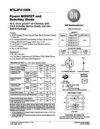
NTLJF4156N Power MOSFET and Schottky Diode 30 V, 4.6 A, mCool] N-Channel, with 2.0 A Schottky Barrier Diode, 2x2 mm http //onsemi.com WDFN Package MOSFET Features V(BR)DSS RDS(on) MAX ID MAX (Note 1) WDFN Package Provides Exposed Drain Pad for Excellent Thermal Conduction 70 mW @ 4.5 V Co-Packaged MOSFET and Schottky For Easy Circuit Layout 30 V 90 mW @ 2.5 V 4.6 A RD... See More ⇒
ntljf4156n.pdf
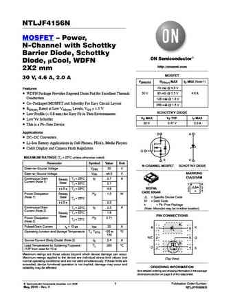
NTLJF4156N MOSFET Power, N-Channel with Schottky Barrier Diode, Schottky Diode, mCool, WDFN http //onsemi.com 2X2 mm MOSFET 30 V, 4.6 A, 2.0 A V(BR)DSS RDS(on) MAX ID MAX (Note 1) 70 mW @ 4.5 V Features 30 V 90 mW @ 2.5 V 4.6 A WDFN Package Provides Exposed Drain Pad for Excellent Thermal Conduction 125 mW @ 1.8 V Co-Packaged MOSFET and Schottky For Easy Circuit Layo... See More ⇒
ntljf3117p-d ntljf3117pt1g ntljf3117ptag.pdf
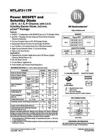
NTLJF3117P Power MOSFET and Schottky Diode -20 V, -4.1 A, P-Channel, with 2.0 A Schottky Barrier Diode, 2x2 mm, mCool] Package http //onsemi.com Features MOSFET FETKYt Configuration with MOSFET plus Low Vf Schottky Diode mCOOLt Package Provides Exposed Drain Pad for Excellent V(BR)DSS RDS(on) MAX ID MAX (Note 1) Thermal Conduction 100 mW @ -4.5 V 2x2 mm Footprint Same ... See More ⇒
ntljf3118n ntljf3118ntag.pdf
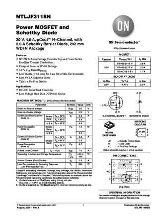
NTLJF3118N Power MOSFET and Schottky Diode 20 V, 4.6 A, mCool] N-Channel, with 2.0 A Schottky Barrier Diode, 2x2 mm http //onsemi.com WDFN Package MOSFET Features V(BR)DSS RDS(on) Max ID Max WDFN 2x2 mm Package Provides Exposed Drain Pad for Excellent Thermal Conduction 65 mW @ 4.5 V 3.8 A Footprint Same as SC-88 Package 20 V 85 mW @ 2.5 V 2.0 A 1.8 V VGS Rated RDS(o... See More ⇒

Detailed specifications: NTLJD3119CTAG, NTLJD3119CTBG, NTLJD3182FZTAG, NTLJD3182FZTBG, NTLJF3117PT1G, NTLJF3117PTAG, NTLJF3118NTAG, NTLJF4156NT1G, IRLZ44N, NTLJS1102PTAG, NTLJS1102PTBG, NTLJS2103PTAG, NTLJS2103PTBG, NTLJS3113PT1G, NTLJS3113PTAG, NTLJS3180PZTBG, NTLJS3A18PZ
Keywords - NTLJF4156NTAG MOSFET specs
NTLJF4156NTAG cross reference
NTLJF4156NTAG equivalent finder
NTLJF4156NTAG pdf lookup
NTLJF4156NTAG substitution
NTLJF4156NTAG replacement
Learn how to find the right MOSFET substitute. A guide to cross-reference, check specs and replace MOSFETs in your circuits.
🌐 : EN ES РУ

LIST
Last Update
MOSFET: BCD70N07A | BCD90N03 | BCD80N06 | T50N06 | H50N06 | BCD12N65 | BCT12N65 | BCD4N65 | BCT4N65 | BCD7N65
Popular searches
c3852 | irfp140 | ksc2383 datasheet | 2n3906 equivalent | a733 transistor equivalent | 2n5401 transistor datasheet | 2n2222 data sheet | irf3205 datasheet