NTLJS4159NT1G Specs and Replacement
Type Designator: NTLJS4159NT1G
Type of Transistor: MOSFET
Type of Control Channel: N-Channel
Absolute Maximum Ratings
Pd ⓘ - Maximum Power Dissipation: 0.7 W
|Vds|ⓘ - Maximum Drain-Source Voltage: 30 V
|Vgs|ⓘ - Maximum Gate-Source Voltage: 8 V
|Id| ⓘ - Maximum Drain Current: 3.6 A
Tj ⓘ - Maximum Junction Temperature: 150 °C
Electrical Characteristics
tr ⓘ - Rise Time: 12.4 nS
Cossⓘ - Output Capacitance: 115.5 pF
Rds ⓘ - Maximum Drain-Source On-State Resistance: 0.035 Ohm
Package: WDFN6
NTLJS4159NT1G substitution
- MOSFET ⓘ Cross-Reference Search
NTLJS4159NT1G datasheet
ntljs4159n ntljs4159nt1g.pdf
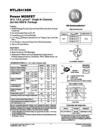
NTLJS4159N Power MOSFET 30 V, 7.8 A, mCoolt Single N-Channel, 2x2 mm WDFN Package Features WDFN Package Provides Exposed Drain Pad for Excellent Thermal http //onsemi.com Conduction 2x2 mm Footprint Same as SC-88 V(BR)DSS RDS(on) MAX ID MAX (Note 1) Lowest RDS(on) in 2x2 mm Package 35 mW @ 4.5 V 1.8 V RDS(on) Rating for Operation at Low Voltage Logic Level Gate 30 V... See More ⇒
ntljs4114n.pdf
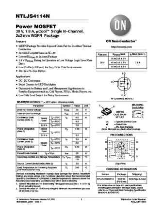
NTLJS4114N Power MOSFET 30 V, 7.8 A, mCoolt Single N-Channel, 2x2 mm WDFN Package Features WDFN Package Provides Exposed Drain Pad for Excellent Thermal http //onsemi.com Conduction 2x2 mm Footprint Same as SC-88 V(BR)DSS RDS(on) MAX ID MAX (Note 1) Lowest RDS(on) in 2x2 mm Package 35 mW @ 4.5 V 1.8 V RDS(on) Rating for Operation at Low Voltage Logic Level Gate 30 V... See More ⇒
ntljs4149 ntljs4149ptag.pdf
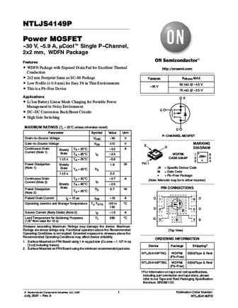
NTLJS4149P Power MOSFET -30 V, -5.9 A, mCoolt Single P-Channel, 2x2 mm, WDFN Package Features WDFN Package with Exposed Drain Pad for Excellent Thermal http //onsemi.com Conduction 2x2 mm Footprint Same as SC-88 Package V(BR)DSS RDS(on) MAX Low Profile (... See More ⇒
ntljs4114nt1g.pdf
NTLJS4114N Power MOSFET 30 V, 7.8 A, mCoolt Single N-Channel, 2x2 mm WDFN Package Features WDFN Package Provides Exposed Drain Pad for Excellent Thermal http //onsemi.com Conduction 2x2 mm Footprint Same as SC-88 V(BR)DSS RDS(on) MAX ID MAX (Note 1) Lowest RDS(on) in 2x2 mm Package 35 mW @ 4.5 V 1.8 V RDS(on) Rating for Operation at Low Voltage Logic Level Gate 30 V ... See More ⇒
Detailed specifications: NTLJS2103PTAG , NTLJS2103PTBG , NTLJS3113PT1G , NTLJS3113PTAG , NTLJS3180PZTBG , NTLJS3A18PZ , NTLJS4114NT1G , NTLJS4149PTAG , P55NF06 , NTLLD4901NF , NTLUD3A260PZTAG , NTLUD3A260PZTBG , NTLUD3A50PZ , NTLUD4C26N , NTLUF4189NZTAG , NTLUS3A18PZ , NTLUS3A18PZTAG .
Keywords - NTLJS4159NT1G MOSFET specs
NTLJS4159NT1G cross reference
NTLJS4159NT1G equivalent finder
NTLJS4159NT1G pdf lookup
NTLJS4159NT1G substitution
NTLJS4159NT1G replacement
Step-by-step guide to finding a MOSFET replacement. Cross-reference parts and ensure compatibility for your repair or project.


LIST
Last Update
MOSFET: AOTF20N40L | AOTF11N60L | AOT11N60L | AONS21303C | AOI280A60 | AOB66914L | AO3485C | AOI780A70 | AOB42S60L | AOTF950A70L
Popular searches
2sc2312 | bu406 datasheet | irfb7437 | tip32a | p75nf75 mosfet equivalent | irfpe50 | tip50 | transistor bc547 datasheet