NTMS4916NR2G Datasheet. Specs and Replacement
Type Designator: NTMS4916NR2G 📄📄
Marking Code: 4916N
Type of Transistor: MOSFET
Type of Control Channel: N-Channel
Absolute Maximum Ratings
Pd ⓘ - Maximum Power Dissipation: 0.89 W
|Vds|ⓘ - Maximum Drain-Source Voltage: 30 V
|Vgs|ⓘ - Maximum Gate-Source Voltage: 20 V
|Id| ⓘ - Maximum Drain Current: 7.8 A
Tj ⓘ - Maximum Junction Temperature: 150 °C
Electrical Characteristics
|VGSth|ⓘ - Maximum Gate-Threshold Voltage: 2.5 V
Qg ⓘ - Total Gate Charge: 15 nC
tr ⓘ - Rise Time: 7.4 nS
Cossⓘ - Output Capacitance: 401 pF
RDSonⓘ - Maximum Drain-Source On-State Resistance: 0.009 Ohm
Package: SO-8
NTMS4916NR2G substitution
- MOSFET ⓘ Cross-Reference Search
NTMS4916NR2G datasheet
ntms4916nr2g.pdf
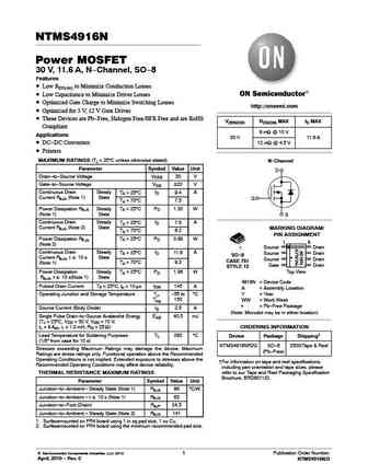
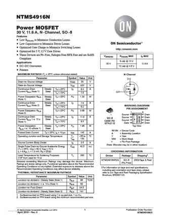
NTMS4916N Power MOSFET 30 V, 11.6 A, N-Channel, SO-8 Features Low RDS(on) to Minimize Conduction Losses Low Capacitance to Minimize Driver Losses Optimized Gate Charge to Minimize Switching Losses http //onsemi.com Optimized for 5 V, 12 V Gate Drives These Devices are Pb-Free, Halogen Free/BFR Free and are RoHS V(BR)DSS RDS(ON) MAX ID MAX Compliant 9 mW @ 10 V A... See More ⇒
ntms4916n.pdf
NTMS4916N Power MOSFET 30 V, 11.6 A, N-Channel, SO-8 Features Low RDS(on) to Minimize Conduction Losses Low Capacitance to Minimize Driver Losses Optimized Gate Charge to Minimize Switching Losses http //onsemi.com Optimized for 5 V, 12 V Gate Drives These Devices are Pb-Free, Halogen Free/BFR Free and are RoHS V(BR)DSS RDS(ON) MAX ID MAX Compliant 9 mW @ 10 V A... See More ⇒
ntms4917n.pdf

NTMS4917N Power MOSFET 30 V, 10.5 A, N-Channel, SO-8 Features Low RDS(on) to Minimize Conduction Losses Low Capacitance to Minimize Driver Losses Optimized Gate Charge to Minimize Switching Losses http //onsemi.com Optimized for 5 V, 12 V Gate Drives These Devices are Pb-Free, Halogen Free/BFR Free and are RoHS V(BR)DSS RDS(ON) MAX ID MAX Compliant 11 mW @ 10 V ... See More ⇒
ntms4917nr2g.pdf

NTMS4917N Power MOSFET 30 V, 10.5 A, N-Channel, SO-8 Features Low RDS(on) to Minimize Conduction Losses Low Capacitance to Minimize Driver Losses Optimized Gate Charge to Minimize Switching Losses http //onsemi.com Optimized for 5 V, 12 V Gate Drives These Devices are Pb-Free, Halogen Free/BFR Free and are RoHS V(BR)DSS RDS(ON) MAX ID MAX Compliant 11 mW @ 10 V ... See More ⇒
Detailed specifications: NTMS4706NR2G, NTMS4800NR2G, NTMS4801NR2G, NTMS4802NR2G, NTMS4807NR2G, NTMS4816NR2G, NTMS4872NR2G, NTMS4873NFR2G, SI2302, NTMS4917NR2G, NTMS4937NR2G, NTMS4939NR2G, NTMS4N01R2G, NTMS4P01R2, NTMS5835NLR2G, NTMS5838NLR2G, NTMS5P02R2G
Keywords - NTMS4916NR2G MOSFET specs
NTMS4916NR2G cross reference
NTMS4916NR2G equivalent finder
NTMS4916NR2G pdf lookup
NTMS4916NR2G substitution
NTMS4916NR2G replacement
Can't find your MOSFET? Learn how to find a substitute transistor by analyzing voltage, current and package compatibility
History: NTMS4816NR2G | HMS15N70I | HMS15N70B | IXFT30N60P
🌐 : EN ES РУ

LIST
Last Update
MOSFET: BCD70N07A | BCD90N03 | BCD80N06 | T50N06 | H50N06 | BCD12N65 | BCT12N65 | BCD4N65 | BCT4N65 | BCD7N65
Popular searches
hy3210 | d313 transistor equivalent | 2sb827 | c5200 datasheet | 2n2614 | 2sa777 replacement | 2sc828 transistor | 2sd357