5N90AF Specs and Replacement
Type Designator: 5N90AF
Type of Transistor: MOSFET
Type of Control Channel: N-Channel
Absolute Maximum Ratings
Pd ⓘ - Maximum Power Dissipation: 38 W
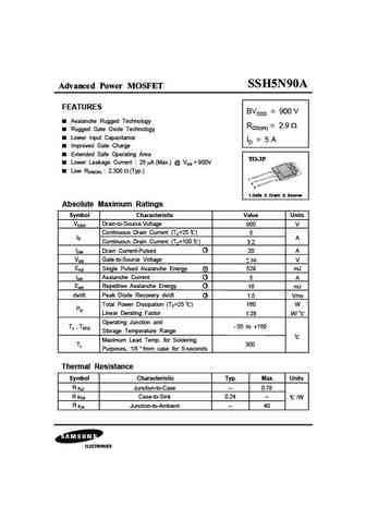
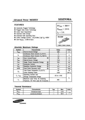
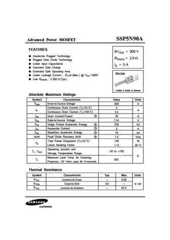
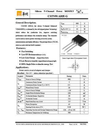
|Vds|ⓘ - Maximum Drain-Source Voltage: 900 V
|Vgs|ⓘ - Maximum Gate-Source Voltage: 30 V
|Id| ⓘ - Maximum Drain Current: 5 A
Tj ⓘ - Maximum Junction Temperature: 150 °C
Electrical Characteristics
tr ⓘ - Rise Time: 65 nS
Cossⓘ - Output Capacitance: 110 pF
RDSonⓘ - Maximum Drain-Source On-State Resistance: 2.8 Ohm
Package: TO-220F
5N90AF substitution
- MOSFET ⓘ Cross-Reference Search
5N90AF datasheet
5n90a 5n90af.pdf
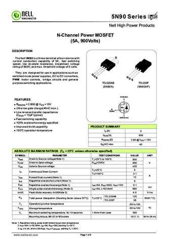
RoHS 5N90 Series RoHS SEMICONDUCTOR Nell High Power Products N-Channel Power MOSFET (5A, 900Volts) DESCRIPTION D The Nell 5N90 is a three-terminal silicon device with current conduction capability of 5A, fast switching speed, low on-state resistance, breakdown voltage rating of 900V, and max. threshold voltage of 5 volts. They are designed for use in applications such as G s... See More ⇒
ssp5n90a.pdf
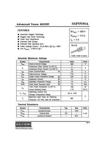
SSP5N90A Advanced Power MOSFET FEATURES BVDSS = 900 V Avalanche Rugged Technology RDS(on) = 2.9 Rugged Gate Oxide Technology Lower Input Capacitance ID = 5 A Improved Gate Charge Extended Safe Operating Area TO-220 Lower Leakage Current 25 A (Max.) @ VDS = 900V Low RDS(ON) 2.300 (Typ.) 1 2 3 1.Gate 2. Drain 3. Source Absolute Maximum Ratings Symbol Chara... See More ⇒
Detailed specifications: 5N60A , 5N60AF , 5N60G , 5N65A , 5N65AF , 5N65F , 5N65G , 5N90A , 4N60 , 65N06A , 65N06H , 6680A , 6HP04CH , 6HP04MH , 6LN04SS , 6N60A , 6N60AF .
History: AP9992GR-HF
Keywords - 5N90AF MOSFET specs
5N90AF cross reference
5N90AF equivalent finder
5N90AF pdf lookup
5N90AF substitution
5N90AF replacement
Step-by-step guide to finding a MOSFET replacement. Cross-reference parts and ensure compatibility for your repair or project.
