IPB067N08N3 Specs and Replacement
Type Designator: IPB067N08N3
Type of Transistor: MOSFET
Type of Control Channel: N-Channel
Absolute Maximum Ratings
Pd ⓘ - Maximum Power Dissipation: 136 W
|Vds|ⓘ - Maximum Drain-Source Voltage: 80 V
|Vgs|ⓘ - Maximum Gate-Source Voltage: 20 V
|Id| ⓘ - Maximum Drain Current: 80 A
Tj ⓘ - Maximum Junction Temperature: 175 °C
Electrical Characteristics
tr ⓘ - Rise Time: 66 nS
Cossⓘ - Output Capacitance: 780 pF
RDSonⓘ - Maximum Drain-Source On-State Resistance: 0.0067 Ohm
IPB067N08N3 substitution
- MOSFET ⓘ Cross-Reference Search
IPB067N08N3 datasheet
ipp070n08n3 ipp070n08n3 ipi070n08n3 ipb067n08n3.pdf
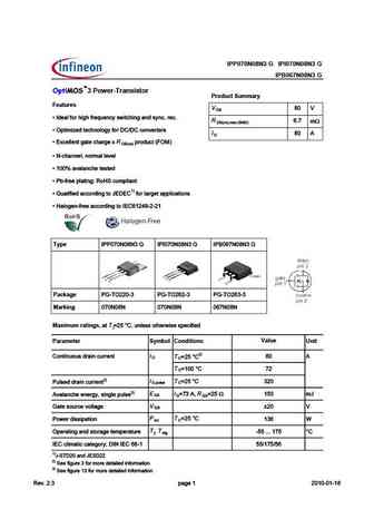
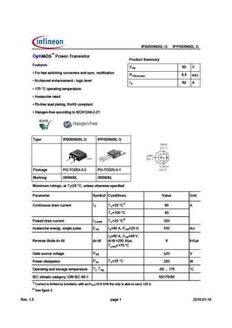
IPP070N08N3 G IPI070N08N3 G IPB067N08N3 G 3 Power-Transistor Product Summary Features V D Q #4513I CG9D389>7 1>4 CI>3 B53 R 7 m , ?> =1H ,& Q ( @D9=9J54 D538>?F5BD5BC I D Q H35>5?B=1... See More ⇒
ipb067n08n3.pdf
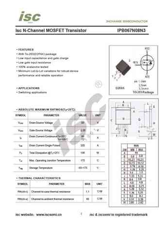
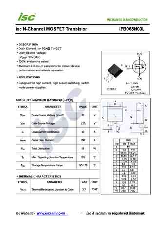
Isc N-Channel MOSFET Transistor IPB067N08N3 FEATURES With To-263(D2PAK) package Low input capacitance and gate charge Low gate input resistance 100% avalanche tested Minimum Lot-to-Lot variations for robust device performance and reliable operation APPLICATIONS Switching applications ABSOLUTE MAXIMUM RATINGS(T =25 ) a SYMBOL PARAMETER VALUE UNIT V Drain-Source V... See More ⇒
ipp070n08n3g ipi070n08n3g ipb067n08n3g.pdf

IPP070N08N3 G IPI070N08N3 G IPB067N08N3 G 3 Power-Transistor Product Summary Features V D Q #4513I CG9D389>7 1>4 CI>3 B53 R 7 m , ?> =1H ,& Q ( @D9=9J54 D538>?F5BD5BC I D Q H35>5?B=1... See More ⇒
ipb06cn10n-g ipi06cn10n-g ipp06cn10n-g.pdf
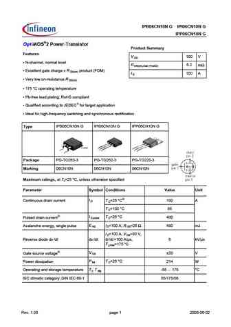
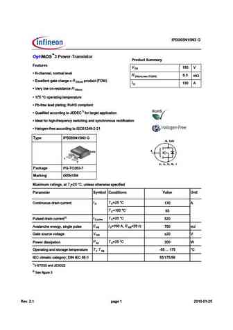
IPB06CN10N G IPI06CN10N G IPP06CN10N G OptiMOS 2 Power-Transistor Product Summary Features V 100 V DS N-channel, normal level R 6.2 m DS(on),max (TO263) Excellent gate charge x R product (FOM) DS(on) I 100 A D Very low on-resistance R DS(on) 175 C operating temperature Pb-free lead plating; RoHS compliant Qualified according to JEDEC1) for target... See More ⇒

Detailed specifications: IPB037N06N3 , IPB039N04L , IPB041N04N , IPB049N06L3 , IPB049NE7N3 , IPB054N06N3 , IPB05CN10N , IPB065N10N3 , IRFZ44N , IPB081N06L3 , IPB083N10N3 , IPB083N15N5LF , IPB097N08N3 , IPB107N20N3 , IPB110N20N3LF , IPB26CN10N , IPB34CN10N .
Keywords - IPB067N08N3 MOSFET specs
IPB067N08N3 cross reference
IPB067N08N3 equivalent finder
IPB067N08N3 pdf lookup
IPB067N08N3 substitution
IPB067N08N3 replacement
Learn how to find the right MOSFET substitute. A guide to cross-reference, check specs and replace MOSFETs in your circuits.
🌐 : EN ES РУ

LIST
Last Update
MOSFET: ASB80R750E | ASB70R380E | ASB65R300E | ASB65R220E | ASB65R120EFD | ASB60R150E | ASA80R900E | ASA80R750E | ASA80R290E | ASA70R950E
Popular searches
lm317t datasheet | irf540 | bc337 | ksc1845 | c1815 transistor | 2sc1815 | irfz44 | 2n5551