DMN6140LQ Specs and Replacement
Type Designator: DMN6140LQ
Type of Transistor: MOSFET
Type of Control Channel: N-Channel
Absolute Maximum Ratings
Pd ⓘ - Maximum Power Dissipation: 0.7 W
|Vds|ⓘ - Maximum Drain-Source Voltage: 60 V
|Vgs|ⓘ - Maximum Gate-Source Voltage: 20 V
|Id| ⓘ - Maximum Drain Current: 1.6 A
Tj ⓘ - Maximum Junction Temperature: 150 °C
Electrical Characteristics
tr ⓘ - Rise Time: 3.6 nS
Cossⓘ - Output Capacitance: 18 pF
RDSonⓘ - Maximum Drain-Source On-State Resistance: 0.14 Ohm
Package: SOT-23
DMN6140LQ substitution
- MOSFET ⓘ Cross-Reference Search
DMN6140LQ datasheet
dmn6140lq.pdf
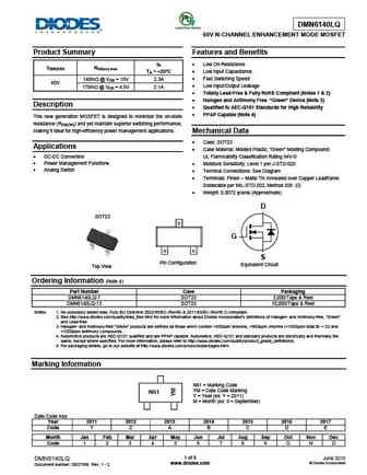
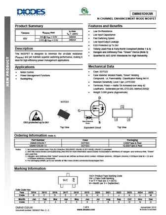
DMN6140LQ 60V N-CHANNEL ENHANCEMENT MODE MOSFET Product Summary Features and Benefits ID Low On-Resistance V(BR)DSS RDS(on) max TA = +25 C Low Input Capacitance Fast Switching Speed 140m @ VGS = 10V 2.3A 60V Low Input/Output Leakage 170m @ VGS = 4.5V 2.1A Totally Lead-Free & Fully RoHS Compliant (Notes 1 & 2) Halogen and Antimony Free. G... See More ⇒
dmn6140l.pdf
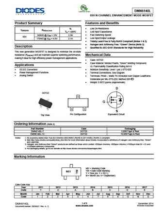
DMN6140L 60V N-CHANNEL ENHANCEMENT MODE MOSFET Product Summary Features and Benefits ID Low On-Resistance V(BR)DSS RDS(on) max TA = +25 C Low Input Capacitance Fast Switching Speed 140m @ VGS = 10V 2.3A 60V Low Input/Output Leakage 170m @ VGS = 4.5V 2.1A Totally Lead-Free & Fully RoHS Compliant (Notes 1 & 2) Halogen and Antimony Free. Gr... See More ⇒
dmn61d8l dmn61d8lvt.pdf
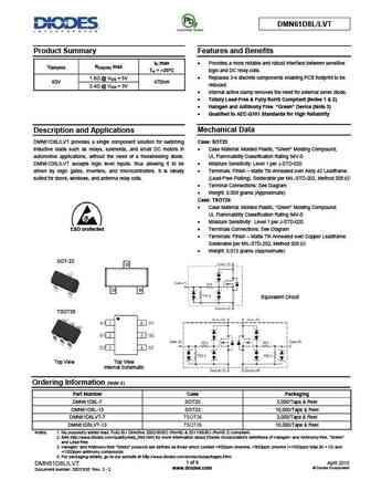
DMN61D8L/LVT Product Summary Features and Benefits ID max Provides a more reliable and robust interface between sensitive V(BR)DSS RDS(ON) max TA = +25 C logic and DC relay coils. Replaces 3-4 discrete components enabling PCB footprint to be 1.8 @ VGS = 5V 60V 470mA reduced. 2.4 @ VGS = 3V Internal active clamp removes the need for external zener diode. ... See More ⇒
dmn61d8lq.pdf
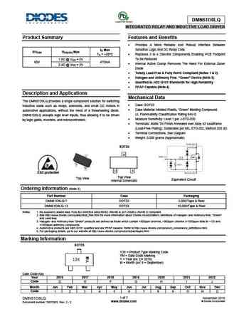
DMN61D8LQ INTEGRATED RELAY AND INDUCTIVE LOAD DRIVER Product Summary Features and Benefits Provides A More Reliable And Robust Interface Between ID Max Sensitive Logic And DC Relay Coils BVDSS RDS(ON) Max TA = +25 Replaces 3 to 4 Discrete Components Enabling PCB Footprint C To Be Reduced 1.8 @ VGS = 5V 60V 470mA Internal Active Clamp Removes The Need For E... See More ⇒
Detailed specifications: DMN6040SSD, DMN6040SSS, DMN6040SVT, DMN6069SE, DMN6070SFCL, DMN6070SSD, DMN6075S, DMN6140L, IRFP064N, DMN62D0LFB, DMN62D0LFD, DMN62D0SFD, DMN62D1LFD, DMN63D8LDW, DMN63D8LV, DMN65D8L, DMN65D8LDW
Keywords - DMN6140LQ MOSFET specs
DMN6140LQ cross reference
DMN6140LQ equivalent finder
DMN6140LQ pdf lookup
DMN6140LQ substitution
DMN6140LQ replacement
Need a MOSFET replacement? Our guide shows you how to find a perfect substitute by comparing key parameters and specs
🌐 : EN ES РУ
LIST
Last Update
MOSFET: FTF30P35D | FTF25N35DHVT | FTF15N35D | FTE15C35G | FTP02P15G | FTE02P15G | AKF30N5P0SX | AKF30N10S | AKF20P45D | CM4407
Popular searches
irf540z | ss8550 transistor | irfp240 mosfet | tip141 | 2n404 | 2n4250 | d882 transistor equivalent | 17n80c3
