36N06 Specs and Replacement
Type Designator: 36N06
Type of Transistor: MOSFET
Type of Control Channel: N-Channel
Absolute Maximum Ratings
Pd ⓘ
- Maximum Power Dissipation: 120 W
|Vds|ⓘ - Maximum Drain-Source Voltage: 60 V
|Vgs|ⓘ - Maximum Gate-Source Voltage: 15 V
|Id| ⓘ - Maximum Drain Current: 36 A
Tj ⓘ - Maximum Junction Temperature: 175 °C
Electrical Characteristics
RDSonⓘ - Maximum Drain-Source On-State Resistance: 0.04 Ohm
Package: TO-252
- MOSFET ⓘ Cross-Reference Search
36N06 datasheet
..1. Size:242K inchange semiconductor
36n06.pdf 
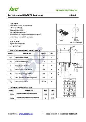
isc N-Channel MOSFET Transistor 36N06 FEATURES Static drain-source on-resistance RDS(on) 40m Enhancement mode 100% avalanche tested Minimum Lot-to-Lot variations for robust device performance and reliable operation DESCRITION High current capability Low gate charge ABSOLUTE MAXIMUM RATINGS(T =25 ) a SYMBOL PARAMETER VALUE UNIT V Drain-Source Voltage 60 V... See More ⇒
0.1. Size:210K motorola
mtb36n06v.pdf

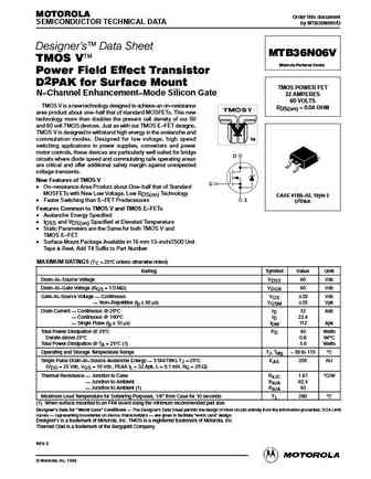
MOTOROLA Order this document SEMICONDUCTOR TECHNICAL DATA by MTB36N06V/D Designer's Data Sheet MTB36N06V TMOS V Motorola Preferred Device Power Field Effect Transistor D2PAK for Surface Mount TMOS POWER FET N Channel Enhancement Mode Silicon Gate 32 AMPERES 60 VOLTS TMOS V is a new technology designed to achieve an on resistance RDS(on) = 0.04 OHM area product about o... See More ⇒
0.2. Size:165K motorola
mtp36n06v.pdf
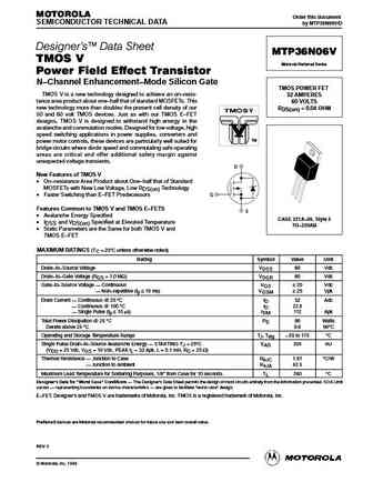
MOTOROLA Order this document SEMICONDUCTOR TECHNICAL DATA by MTP36N06V/D Designer's Data Sheet MTP36N06V TMOS V Motorola Preferred Device Power Field Effect Transistor N Channel Enhancement Mode Silicon Gate TMOS POWER FET TMOS V is a new technology designed to achieve an on resis- 32 AMPERES tance area product about one half that of standard MOSFETs. This 60 VOLTS n... See More ⇒
0.3. Size:188K motorola
mtp36n06v .pdf

MOTOROLA Order this document SEMICONDUCTOR TECHNICAL DATA by MTP36N06V/D Designer's Data Sheet MTP36N06V TMOS V Motorola Preferred Device Power Field Effect Transistor N Channel Enhancement Mode Silicon Gate TMOS POWER FET TMOS V is a new technology designed to achieve an on resis- 32 AMPERES tance area product about one half that of standard MOSFETs. This 60 VOLTS n... See More ⇒
0.4. Size:278K motorola
mtb36n06erev0.pdf
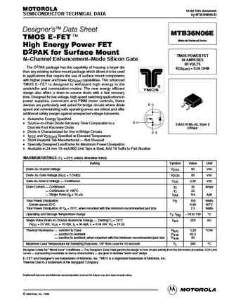
MOTOROLA Order this document SEMICONDUCTOR TECHNICAL DATA by MTB36N06E/D Designer's Data Sheet MTB36N06E TMOS E-FET. Motorola Preferred Device High Energy Power FET D2PAK for Surface Mount TMOS POWER FET N Channel Enhancement Mode Silicon Gate 36 AMPERES 60 VOLTS The D2PAK package has the capability of housing a larger die RDS(on) = 0.04 OHM than any existing surface mo... See More ⇒
0.5. Size:241K motorola
mtb36n06vrev2x.pdf
MOTOROLA Order this document SEMICONDUCTOR TECHNICAL DATA by MTB36N06V/D Designer's Data Sheet MTB36N06V TMOS V Motorola Preferred Device Power Field Effect Transistor D2PAK for Surface Mount TMOS POWER FET N Channel Enhancement Mode Silicon Gate 32 AMPERES 60 VOLTS TMOS V is a new technology designed to achieve an on resistance RDS(on) = 0.04 OHM area product about o... See More ⇒
0.6. Size:239K motorola
mtb36n06e.pdf

MOTOROLA Order this document SEMICONDUCTOR TECHNICAL DATA by MTB36N06E/D Designer's Data Sheet MTB36N06E TMOS E-FET. Motorola Preferred Device High Energy Power FET D2PAK for Surface Mount TMOS POWER FET N Channel Enhancement Mode Silicon Gate 36 AMPERES 60 VOLTS The D2PAK package has the capability of housing a larger die RDS(on) = 0.04 OHM than any existing surface mo... See More ⇒
0.7. Size:54K philips
phb36n06e 1.pdf
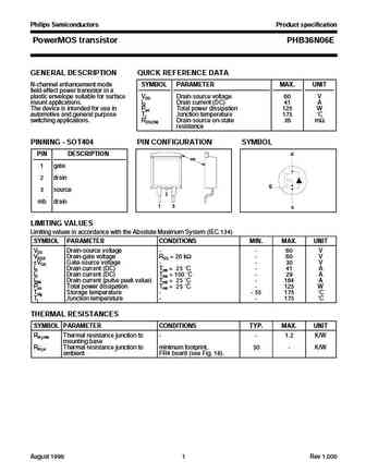
Philips Semiconductors Product specification PowerMOS transistor PHB36N06E GENERAL DESCRIPTION QUICK REFERENCE DATA N-channel enhancement mode SYMBOL PARAMETER MAX. UNIT field-effect power transistor in a plastic envelope suitable for surface VDS Drain-source voltage 60 V mount applications. ID Drain current (DC) 41 A The device is intended for use in Ptot Total power dissipation 125 W... See More ⇒
0.8. Size:51K philips
php36n06e.pdf
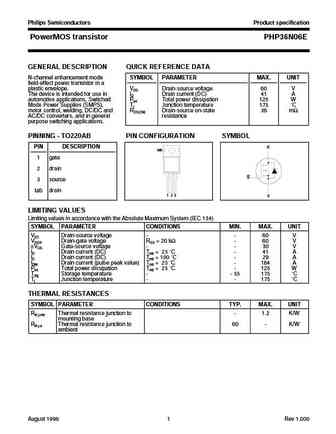
Philips Semiconductors Product specification PowerMOS transistor PHP36N06E GENERAL DESCRIPTION QUICK REFERENCE DATA N-channel enhancement mode SYMBOL PARAMETER MAX. UNIT field-effect power transistor in a plastic envelope. VDS Drain-source voltage 60 V The device is intended for use in ID Drain current (DC) 41 A automotive applications, Switched Ptot Total power dissipation 125 W Mode... See More ⇒
0.9. Size:54K philips
phb36n06e.pdf

Philips Semiconductors Product specification PowerMOS transistor PHB36N06E GENERAL DESCRIPTION QUICK REFERENCE DATA N-channel enhancement mode SYMBOL PARAMETER MAX. UNIT field-effect power transistor in a plastic envelope suitable for surface VDS Drain-source voltage 60 V mount applications. ID Drain current (DC) 41 A The device is intended for use in Ptot Total power dissipation 125 W... See More ⇒
0.10. Size:51K philips
php36n06e 1.pdf

Philips Semiconductors Product specification PowerMOS transistor PHP36N06E GENERAL DESCRIPTION QUICK REFERENCE DATA N-channel enhancement mode SYMBOL PARAMETER MAX. UNIT field-effect power transistor in a plastic envelope. VDS Drain-source voltage 60 V The device is intended for use in ID Drain current (DC) 41 A automotive applications, Switched Ptot Total power dissipation 125 W Mode... See More ⇒
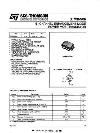
0.11. Size:414K st
stp36n06.pdf
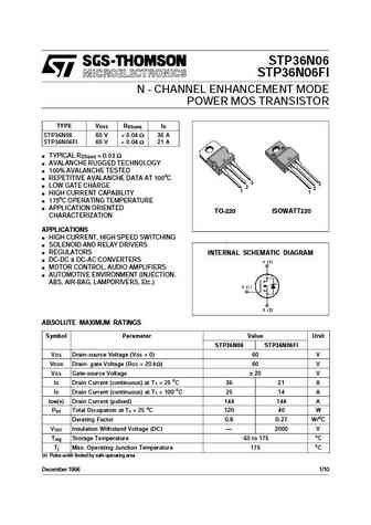
STP36N06 STP36N06FI N - CHANNEL ENHANCEMENT MODE POWER MOS TRANSISTOR TYPE VDSS RDS(on) ID STP36N06 60 V ... See More ⇒
0.13. Size:401K st
stp36n06l.pdf
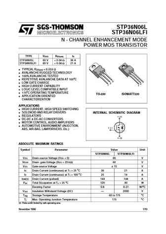
STP36N06L STP36N06LFI N - CHANNEL ENHANCEMENT MODE POWER MOS TRANSISTOR TYPE VDSS RDS(on) ID STP36N05L 60 V ... See More ⇒
0.14. Size:202K onsemi
mtp36n06v.pdf
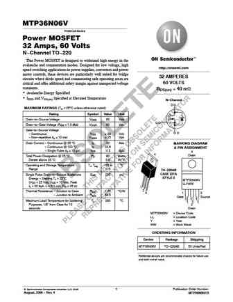
MTP36N06V Preferred Device Power MOSFET 32 Amps, 60 Volts N-Channel TO-220 This Power MOSFET is designed to withstand high energy in the avalanche and commutation modes. Designed for low voltage, high http //onsemi.com speed switching applications in power supplies, converters and power motor controls, these devices are particularly well suited for bridge 32 AMPERES circuits where di... See More ⇒
0.15. Size:370K inpower semi
ftd36n06n.pdf
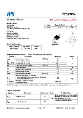
FTD36N06N N-Channel MOSFET Pb Lead Free Package and Finish Applications VDSS RDS(ON) (Typ.) ID Automotive DC Motor Control 60V 28 m 25A DC-DC Converters and Off-Line UPS Features RoHS Compliant D Low ON Resistance D Low Gate Charge Peak Current vs Pulse Width Curve G G S TO-252 Ordering Information Not to Scale S PART NUMBER PACKAGE BRAND ... See More ⇒
0.16. Size:497K stansontech
st36n06.pdf
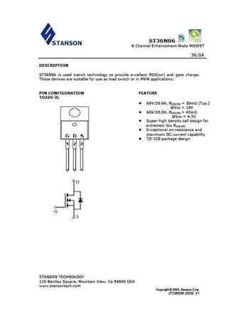
ST36N06 N Channel Enhancement Mode MOSFET 36.0A DESCRIPTION ST36N06 is used trench technology to provide excellent RDS(on) and gate charge. Those devices are suitable for use as load switch or in PWM applications. PIN CONFIGURATION FEATURE TO220-3L 60V/20.0A, RDS(ON) = 30m (Typ.) @VGS = 10V 60V/20.0A, RDS(ON) = 45m @VGS = 4.5V Super high density cell design f... See More ⇒
0.17. Size:737K cn vbsemi
ftu36n06n.pdf
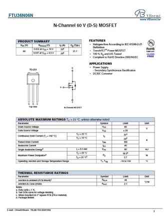
FTU36N06N www.VBsemi.tw N-Channel 60 V (D-S) MOSFET FEATURES PRODUCT SUMMARY Halogen-free According to IEC 61249-2-21 VDS (V) RDS(on) ( ) ID (A) Qg (Typ.) Definition 0.032 at VGS = 10 V 35d TrenchFET Power MOSFET 60 21.7 0.037 at VGS = 4.5 V 30d 100 % Rg and UIS Tested Compliant to RoHS Directive 2002/95/EC APPLICATIONS Power Supply D TO-251 - Seconda... See More ⇒
0.18. Size:711K cn vbsemi
ftd36n06n.pdf
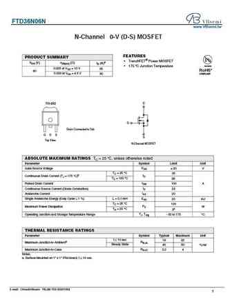
FTD36N06N www.VBsemi.tw N-Channel 6 0-V (D-S) MOSFET FEATURES PRODUCT SUMMARY TrenchFET Power MOSFET VDS (V) rDS(on) ( ) ID (A)a Available 175 C Junction Temperature 0.025 at VGS = 10 V 35 RoHS* 60 0.030 at VGS = 4.5 V 30 COMPLIANT TO-252 D G Drain Connected to Tab G D S S Top View N-Channel MOSFET ABSOLUTE MAXIMUM RATINGS TC = 25 C, unless otherwise n... See More ⇒
Detailed specifications: DSK5J01, DSK5J01X0L, DSK9J01, DSKTJ04, DSKTJ05, DSKTJ07, DSKTJ08, 2SK3591, BS170, 65N06, FCP125N65S3, FKI10300, FMH08N80E, FQU10N20, IPA180N10N3, IPA60R120P7, IPB048N15N5LF
Keywords - 36N06 MOSFET specs
36N06 cross reference
36N06 equivalent finder
36N06 pdf lookup
36N06 substitution
36N06 replacement
Can't find your MOSFET?
Learn how to find a substitute transistor by analyzing voltage, current and package compatibility