IPP200N25N3 Specs and Replacement
Type Designator: IPP200N25N3
Type of Transistor: MOSFET
Type of Control Channel: N-Channel
Absolute Maximum Ratings
Pd ⓘ - Maximum Power Dissipation: 300 W
|Vds|ⓘ - Maximum Drain-Source Voltage: 250 V
|Vgs|ⓘ - Maximum Gate-Source Voltage: 20 V
|Id| ⓘ - Maximum Drain Current: 64 A
Tj ⓘ - Maximum Junction Temperature: 175 °C
Electrical Characteristics
tr ⓘ - Rise Time: 20 nS
Cossⓘ - Output Capacitance: 297 pF
Rds ⓘ - Maximum Drain-Source On-State Resistance: 0.02 Ohm
Package: TO-220
IPP200N25N3 substitution
- MOSFET ⓘ Cross-Reference Search
IPP200N25N3 datasheet
ipp200n25n3.pdf
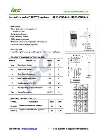
isc N-Channel MOSFET Transistor IPP200N25N3 IIPP200N25N3 FEATURES Static drain-source on-resistance RDS(on) 20m Enhancement mode Fast Switching Speed 100% avalanche tested Minimum Lot-to-Lot variations for robust device performance and reliable operation DESCRITION Ideal for high-frequency switching and synchronous rectification ABSOLUTE MAXIMUM RATINGS(T ... See More ⇒
ipb200n25n3-g ipp200n25n3-g ipi200n25n3-g ipb200n25n3g ipp200n25n3g ipi200n25n3g.pdf
... See More ⇒
ipb200n15n3g ipd200n15n3g ipi200n15n3g ipp200n15n3g ipb200n15n3 ipd200n15n3 ipi200n15n3 ipp200n15n3.pdf
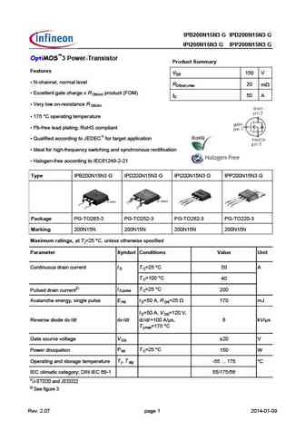
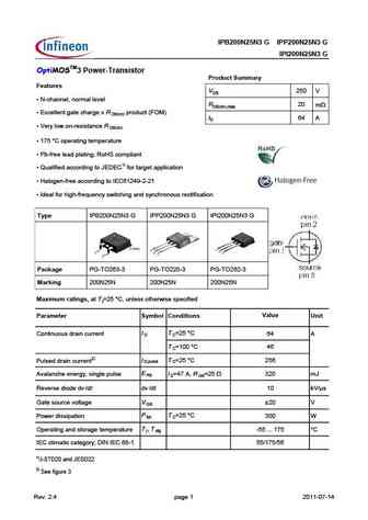
IPB200N15N3 G IPD200N15N3 G IPI200N15N3 G IPP200N15N3 G OptiMOS 3 Power-Transistor Product Summary Features VDS 150 V N-channel, normal level RDS(on),max 20 mW Excellent gate charge x R product (FOM) DS(on) ID 50 A Very low on-resistance R DS(on) 175 C operating temperature Pb-free lead plating; RoHS compliant Qualified according to JEDEC1) for t... See More ⇒
ipp200n15n3.pdf
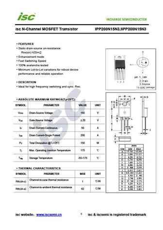
isc N-Channel MOSFET Transistor IPP200N15N3,IIPP200N15N3 FEATURES Static drain-source on-resistance RDS(on) 20m Enhancement mode Fast Switching Speed 100% avalanche tested Minimum Lot-to-Lot variations for robust device performance and reliable operation DESCRITION Ideal for high frequency switching and sync. Rec. ABSOLUTE MAXIMUM RATINGS(T =25 ) a SYMBOL... See More ⇒
Detailed specifications: IPP100N08N3 , IPP110N20N3 , IPP111N15N3 , IPP114N12N3 , IPP12CN10L , IPP147N12N3 , IPP16CN10N , IPP200N15N3 , SKD502T , IPP320N20N3 , IPP530N15N3 , IPP600N25N3 , IPP60R060C7 , IPP60R080P7 , IPP60R099P7 , IPP60R120C7 , IPP60R170CFD7 .
Keywords - IPP200N25N3 MOSFET specs
IPP200N25N3 cross reference
IPP200N25N3 equivalent finder
IPP200N25N3 pdf lookup
IPP200N25N3 substitution
IPP200N25N3 replacement
Need a MOSFET replacement? Our guide shows you how to find a perfect substitute by comparing key parameters and specs


LIST
Last Update
MOSFET: AOTF20N40L | AOTF11N60L | AOT11N60L | AONS21303C | AOI280A60 | AOB66914L | AO3485C | AOI780A70 | AOB42S60L | AOTF950A70L
Popular searches
c644 transistor | fgpf4536 datasheet | p20nm60fp datasheet | 2sc1943 | 7408 mosfet | cs630 | 2sc2705 transistor | 647 transistor