2N6568 Specs and Replacement
Type Designator: 2N6568
Type of Transistor: JFET
Type of Control Channel: N-Channel
Absolute Maximum Ratings
Pd ⓘ - Maximum Power Dissipation: 0.4 W
|Vds|ⓘ - Maximum Drain-Source Voltage: 30 V
|Id| ⓘ - Maximum Drain Current: 1 A
Tj ⓘ - Maximum Junction Temperature: 200 °C
Electrical Characteristics
RDSonⓘ - Maximum Drain-Source On-State Resistance: 2.5 Ohm
Package: TO52
2N6568 substitution
- MOSFET ⓘ Cross-Reference Search
2N6568 datasheet
2n6560.pdf

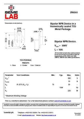
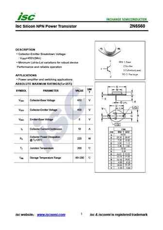
2N6560 Dimensions in mm (inches). Bipolar NPN Device in a Hermetically sealed TO3 25.15 (0.99) 6.35 (0.25) 26.67 (1.05) 9.15 (0.36) Metal Package. 10.67 (0.42) 11.18 (0.44) 1.52 (0.06) 3.43 (0.135) 1 2 Bipolar NPN Device. 3 VCEO = 450V (case) 3.84 (0.151) 4.09 (0.161) 7.92 (0.312) IC = 10A 12.70 (0.50) All Semelab hermetically sealed products can be processed in ... See More ⇒

Detailed specifications: SVS5N70F, SVS5N70MU, WFP85N06, 2N5653, 2N5654, 2N60A, 2N60AF, 2N60G, 8205A, 2N6659-2, 2N6659X, 2N6660-2, 2N6660C4A, 2N6660CSM4, 2N6661-2, 2N6661CSM4, 2N6661DCSM
Keywords - 2N6568 MOSFET specs
2N6568 cross reference
2N6568 equivalent finder
2N6568 pdf lookup
2N6568 substitution
2N6568 replacement
Learn how to find the right MOSFET substitute. A guide to cross-reference, check specs and replace MOSFETs in your circuits.
History: AUIRF7342Q | AOC3864 | NTR1P02LT1G | SM2604NSC | AGM615MNA | CS4N70A3D | IRF7379Q
🌐 : EN ES РУ

LIST
Last Update
MOSFET: AUB034N10 | AUB033N08BG | AUB026N085 | AUA062N08BG | AUA060N08AG | AUA056N08BGL | AUA039N10 | ASW80R290E | ASW65R120EFD | ASW65R110E
Popular searches
fb42n20d | irfb3306 equivalent | irfp460 характеристики | k2837 datasheet | k389 transistor | mje15032g equivalent | nsd134 | 60r190p datasheet