2304 Specs and Replacement
Type Designator: 2304
Type of Transistor: MOSFET
Type of Control Channel: N-Channel
Absolute Maximum Ratings
Pd ⓘ - Maximum Power Dissipation: 0.35 W
|Vds|ⓘ - Maximum Drain-Source Voltage: 30 V
|Vgs|ⓘ - Maximum Gate-Source Voltage: 20 V
|Id| ⓘ - Maximum Drain Current: 3.3 A
Tj ⓘ - Maximum Junction Temperature: 150 °C
Electrical Characteristics
tr ⓘ - Rise Time: 50 nS
Cossⓘ - Output Capacitance: 45 pF
RDSonⓘ - Maximum Drain-Source On-State Resistance: 0.06 Ohm
Package: SOT-23
2304 substitution
- MOSFET ⓘ Cross-Reference Search
2304 datasheet
si2304ds.pdf
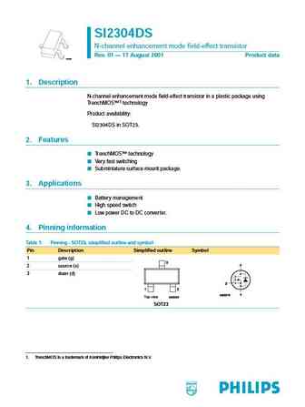
SI2304DS N-channel enhancement mode field-effect transistor Rev. 01 17 August 2001 Product data M3D088 1. Description N-channel enhancement mode field-effect transistor in a plastic package using TrenchMOS 1 technology Product availability SI2304DS in SOT23. 2. Features TrenchMOS technology Very fast switching Subminiature surface mount package. 3. Applications Batte... See More ⇒
msc82304.pdf
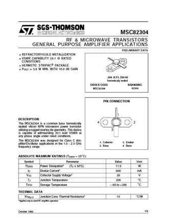
MSC82304 RF & MICROWAVE TRANSISTORS GENERAL PURPOSE AMPLIFIER APPLICATIONS PRELIMINARY DATA .REFRACTORY/GOLD METALLIZATION .VSWR CAPABILITY 20 1 @ RATED CONDITIONS .HERMETIC STRIPAC PACKAGE .P 3.8 W MIN. WITH 10.0 dB GAIN OUT = .250 2LFL (S010) hermetically sealed ORDER CODE BRANDING MSC82304 82304 PIN CONNECTION DESCRIPTION The MSC82304 is a common base hermetically sealed ... See More ⇒
rn2301 rn2302 rn2303 rn2304 rn2305 rn2306.pdf
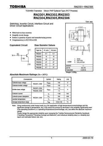
RN2301 RN2306 TOSHIBA Transistor Silicon PNP Epitaxial Type (PCT Process) RN2301,RN2302,RN2303 RN2304,RN2305,RN2306 Unit mm Switching, Inverter Circuit, Interface Circuit and Driver Circuit Applications With built-in bias resistors Simplify circuit design Reduce a quantity of parts and manufacturing process Complementary to RN1301to1306 Equivalent Circuit Bias Resi... See More ⇒
si2304bds.pdf
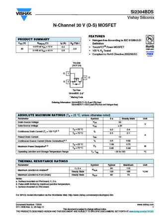
Si2304BDS Vishay Siliconix N-Channel 30 V (D-S) MOSFET FEATURES PRODUCT SUMMARY Halogen-free According to IEC 61249-2-21 VDS (V) RDS(on) ( )ID (A) Qg (Typ.) Definition 0.070 at VGS = 10 V 3.2 TrenchFET Power MOSFET 30 2.6 0.105 at VGS = 4.5 V 2.6 100 % Rg Tested Compliant to RoHS Directive 2002/95/EC TO-236 (SOT-23) G 1 3 D S 2 Top View Si2304BDS ... See More ⇒
si2304dds.pdf
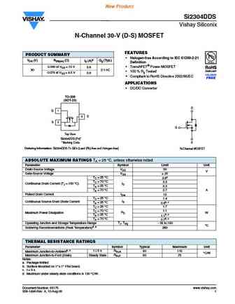
New Product Si2304DDS Vishay Siliconix N-Channel 30-V (D-S) MOSFET FEATURES PRODUCT SUMMARY Halogen-free According to IEC 61249-2-21 VDS (V) RDS(on) ( ) ID (A)a Qg (Typ.) Definition 0.060 at VGS = 10 V TrenchFET Power MOSFET 3.6 30 2.1 nC 100 % Rg Tested 0.075 at VGS = 4.5 V 3.6 Compliant to RoHS Directive 2002/95/EC APPLICATIONS DC/DC Converter T... See More ⇒
si2304dd.pdf

New Product Si2304DDS Vishay Siliconix N-Channel 30-V (D-S) MOSFET FEATURES PRODUCT SUMMARY Halogen-free According to IEC 61249-2-21 VDS (V) RDS(on) ( ) ID (A)a Qg (Typ.) Definition 0.060 at VGS = 10 V TrenchFET Power MOSFET 3.6 30 2.1 nC 100 % Rg Tested 0.075 at VGS = 4.5 V 3.6 Compliant to RoHS Directive 2002/95/EC APPLICATIONS DC/DC Converter T... See More ⇒
si2304ds.pdf
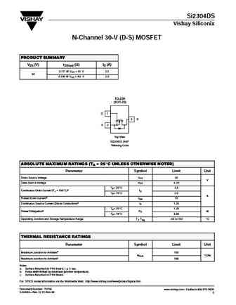
Si2304DS Vishay Siliconix N-Channel 30-V (D-S) MOSFET PRODUCT SUMMARY VDS (V) rDS(on) (W) ID (A) 0.117 @ VGS = 10 V 2.5 30 30 0.190 @ VGS = 4.5 V 2.0 TO-236 (SOT-23) G 1 3 D S 2 Top View Si2304DS (A4)* *Marking Code ABSOLUTE MAXIMUM RATINGS (TA = 25_C UNLESS OTHERWISE NOTED) Parameter Symbol Limit Unit Drain-Source Voltage VDS 30 V V Gate-Source Voltage VGS "20 TA= 25_C 2... See More ⇒
ut2304.pdf
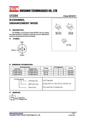
UNISONIC TECHNOLOGIES CO., LTD UT2304 Power MOSFET N-CHANNEL ENHANCEMENT MODE 3 3 1 1 2 2 DESCRIPTION The UT2304 is an N-Channel Power MOSFET that can achieve SOT-23-3 SOT-23 (JEDEC TO-236) (EIAJ SC-59) the lowest possible on-resistance, extremely and cost- effectiveness device by using advanced trench technology. SYMBOL Drain 1 SOT-89 Gate Source ORDERING IN... See More ⇒
cj2304.pdf
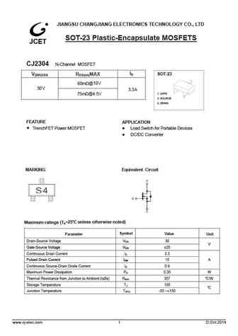
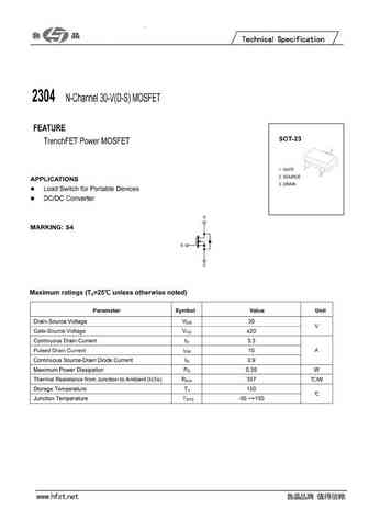
JIANGSU CHANGJIANG ELECTRONICS TECHNOLOGY CO., LTD SOT-23 Plastic-Encapsulate MOSFETS CJ2304 N-Channel MOSFET ID SOT-23 V(BR)DSS RDS(on)MAX 60m @10V 30V 3.3A 1. GATE 75m @4.5V 2. SOURCE 3. DRAIN FEATURE APPLICATION TrenchFET Power MOSFET Load Switch for Portable Devices DC/DC Converter MARKING Equivalent Circuit Maximum ratings (Ta=25 unless other... See More ⇒
se2304.pdf
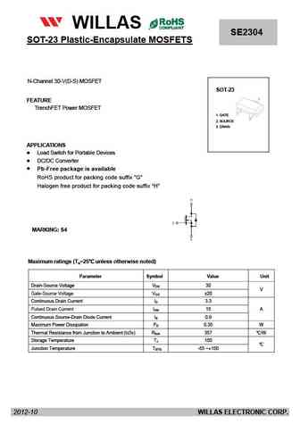
FM120-M WILLAS THRU SE2304 SOT-23 Plastic-Encapsulate MOSFETS FM1200-M 1.0A SURFACE MOUNT SCHOTTKY BARRIER RECTIFIERS -20V- 200V SOD-123 PACKAGE Pb Free Produ Package outline Features Batch process design, excellent power dissipation offers better reverse leakage current and thermal resistance. SOD-123H Low profile surface mounted application in order to N-Channel ... See More ⇒
aons32304.pdf
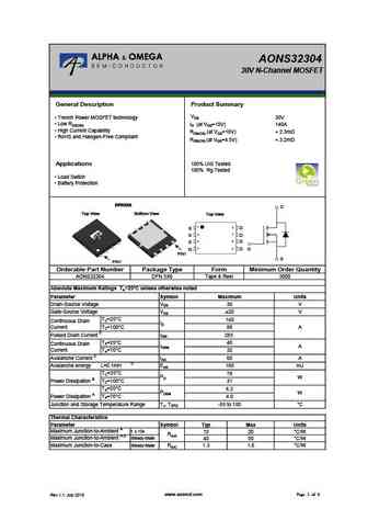
AONS32304 30V N-Channel MOSFET General Description Product Summary VDS Trench Power MOSFET technology 30V Low RDS(ON) ID (at VGS=10V) 140A High Current Capability RDS(ON) (at VGS=10V) ... See More ⇒
ap2304gn-hf.pdf
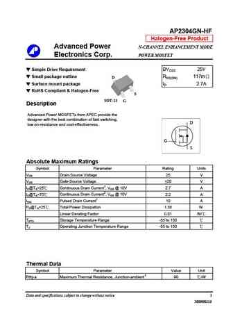
AP2304GN-HF Halogen-Free Product Advanced Power N-CHANNEL ENHANCEMENT MODE Electronics Corp. POWER MOSFET Simple Drive Requirement BVDSS 25V Small package outline RDS(ON) 117m D Surface mount package ID 2.7A RoHS Compliant & Halogen-Free S SOT-23 G Description Advanced Power MOSFETs from APEC provide the designer with the best combination of fast switching, D l... See More ⇒
ap2304agn.pdf
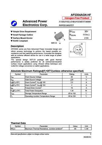
AP2304AGN-HF Halogen-Free Product Advanced Power N-CHANNEL ENHANCEMENT MODE Electronics Corp. POWER MOSFET Simple Drive Requirement BVDSS 30V D Small Package Outline RDS(ON) 117m Surface Mount Device ID 2.5A S RoHS Compliant SOT-23 G D Description AP2304A series are from Advanced Power innovated design and silicon process technology to achieve the lowest possibl... See More ⇒
ap2304gn.pdf
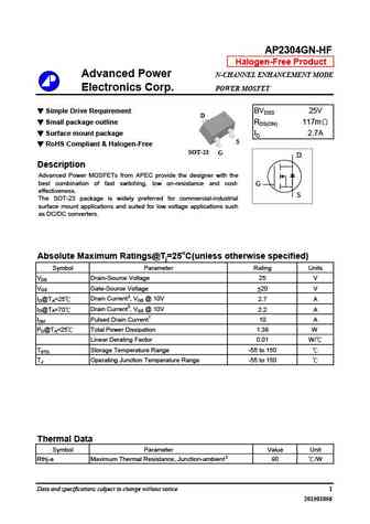
AP2304GN-HF Halogen-Free Product Advanced Power N-CHANNEL ENHANCEMENT MODE Electronics Corp. POWER MOSFET Simple Drive Requirement BVDSS 25V D Small package outline RDS(ON) 117m Surface mount package ID 2.7A S RoHS Compliant & Halogen-Free SOT-23 G D Description Advanced Power MOSFETs from APEC provide the designer with the best combination of fast switching, lo... See More ⇒
ap2304agn-hf.pdf
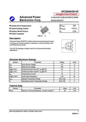
AP2304AGN-HF Halogen-Free Product Advanced Power N-CHANNEL ENHANCEMENT MODE Electronics Corp. POWER MOSFET Simple Drive Requirement BVDSS 30V D Small Package Outline RDS(ON) 117m Surface Mount Device ID 2.5A S RoHS Compliant SOT-23 G Description Advanced Power MOSFETs utilized advanced processing techniques D to achieve the lowest possible on-resistance, extremel... See More ⇒
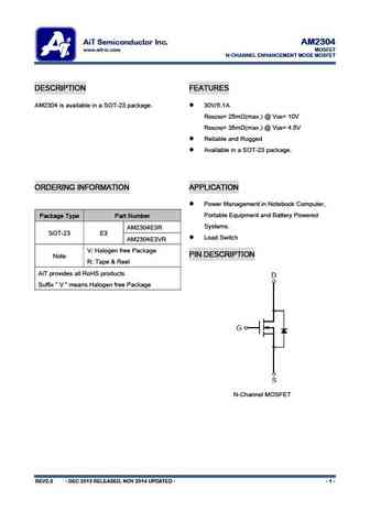
am2304n.pdf
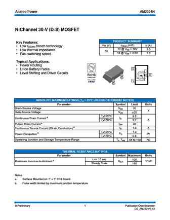
Analog Power AM2304N N-Channel 30-V (D-S) MOSFET PRODUCT SUMMARY Key Features rDS(on) (m ) VDS (V) ID (A) Low r trench technology DS(on) 12 @ VGS = 10V 8.5 Low thermal impedance 30 18 @ VGS = 4.5V 7.0 Fast switching speed Typical Applications Power Routing Li Ion Battery Packs Level Shifting and Driver Circuits ABSOLUTE MAXIMUM RATINGS (TA =... See More ⇒
afn2304s.pdf
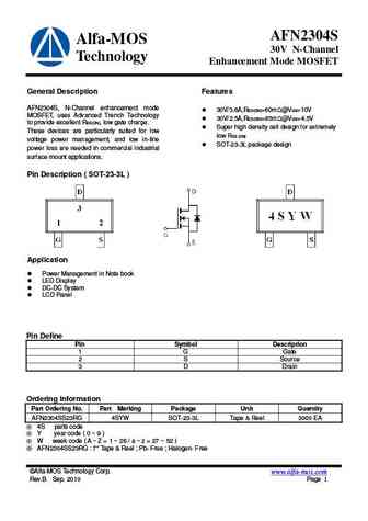
AFN2304S Alfa-MOS 30V N-Channel Technology Enhancement Mode MOSFET General Description Features AFN2304S, N-Channel enhancement mode 30V/3.6A,RDS(ON)=60m @VGS=10V MOSFET, uses Advanced Trench Technology 30V/2.5A,RDS(ON)=85m @VGS=4.5V to provide excellent RDS(ON), low gate charge. Super high density cell design for extremely These devices are particularly suited fo... See More ⇒
afn2304as.pdf
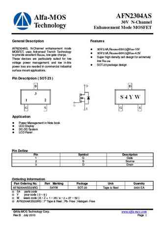
AFN2304AS Alfa-MOS 30V N-Channel Technology Enhancement Mode MOSFET General Description Features AFN2304AS, N-Channel enhancement mode 30V/2.4A,RDS(ON)=65m @VGS=10V MOSFET, uses Advanced Trench Technology 30V/2.0A,RDS(ON)=90m @VGS=4.5V to provide excellent RDS(ON), low gate charge. Super high density cell design for extremely These devices are particularly suited ... See More ⇒
afn2304.pdf

AFN2304 Alfa-MOS 30V N-Channel Technology Enhancement Mode MOSFET General Description Features AFN2304, N-Channel enhancement mode 30V/3.6A,RDS(ON)=78m @VGS=10V MOSFET, uses Advanced Trench Technology 30V/2.8A,RDS(ON)=105m @VGS=4.5V to provide excellent RDS(ON), low gate charge. Super high density cell design for extremely These devices are particularly suited for... See More ⇒
afn2304a.pdf
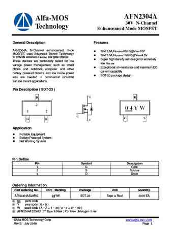
AFN2304A Alfa-MOS 30V N-Channel Technology Enhancement Mode MOSFET General Description Features AFN2304A, N-Channel enhancement mode 30V/2.6A,RDS(ON)=82m @VGS=10V MOSFET, uses Advanced Trench Technology 30V/2.0A,RDS(ON)=108m @VGS=4.5V to provide excellent RDS(ON), low gate charge. Super high density cell design for extremely These devices are particularly suited f... See More ⇒
si2304.pdf
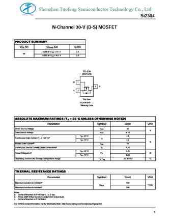
Shenzhen Tuofeng Semiconductor Technology Co., Ltd Si2304 N-Channel 30-V (D-S) MOSFET PRODUCT SUMMARY VDS (V) rDS(on) (W) ID (A) 0.055 @ V 2.5 GS = 10 V 30 30 0.080 @ VGS = 4.5 V 2.0 TO-236 (SOT-23) G 1 3 D S 2 Top View Si2304 (A4)* *Marking Code ABSOLUTE MAXIMUM RATINGS (TA = 25_C UNLESS OTHERWISE NOTED) Parameter Symbol Limit Unit Drain-Source Voltage VDS 30 V V Gate-S... See More ⇒
mtn2304n3.pdf
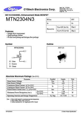
Spec. No. C737N3 Issued Date 2011.11.24 CYStech Electronics Corp. Revised Date 2012.02.10 Page No. 1/8 30V N-CHANNEL Enhancement Mode MOSFET BVDSS 30V MTN2304N3 ID 5A 20m VGS=10V, ID=5A RDSON(TYP) 28m VGS=4.5V, ID=4A Features Simple drive requirement Small package outline Pb-free lead plating and halogen-free package Symbol Outline MTN... See More ⇒
mtn2304m3.pdf
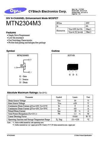
Spec. No. C737M3 Issued Date 2012.07.26 CYStech Electronics Corp. Revised Date 2013.08.12 Page No. 1/8 30V N-CHANNEL Enhancement Mode MOSFET BVDSS 30V MTN2304M3 ID 6A 20m VGS=10V, ID=5A RDSON(TYP) 28m VGS=4.5V, ID=4A Features Single Drive Requirement Low On-resistance Fast Switching Characteristic Pb-free lead plating and halogen-fre... See More ⇒
g2304.pdf
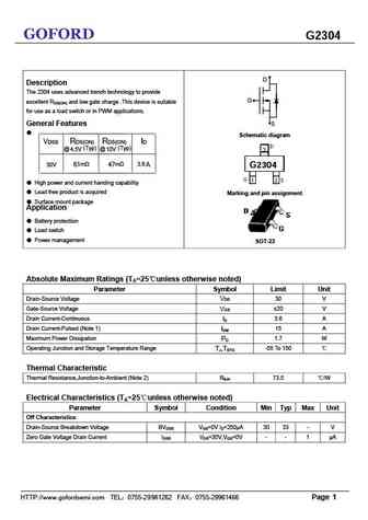
GOFORD G2304 D Description The 2304 uses advanced trench technology to provide G excellent RDS(ON) and low gate charge .This device is suitable for use as a load switch or in PWM applications. General Features S Schematic diagram VDSS RDS(ON) RDS(ON) ID @ 4.5V (Typ) @ 10V (Typ) m m 3.6 30V 61 47 A G2304 High power and current handing capability Lead f... See More ⇒
apm2304a.pdf
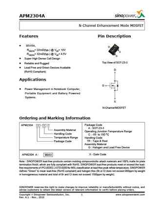
APM2304A N-Channel Enhancement Mode MOSFET Features Pin Description 30V/5A, D RDS(ON)= 22m (typ.) @ VGS= 10V S RDS(ON)= 32m (typ.) @ VGS= 4.5V G Super High Dense Cell Design Top View of SOT-23-3 Reliable and Rugged Lead Free and Green Devices Available D (RoHS Compliant) Applications G Power Management in Notebook Computer, Portable Equipment and Battery Power... See More ⇒
sm2304nsa.pdf
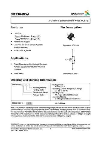
SM2304NSA N-Channel Enhancement Mode MOSFET Features Pin Description 30V/5.1A, D RDS(ON)=25m (max.) @ VGS=10V S RDS(ON)=35m (max.) @ VGS=4.5V G Reliable and Rugged Lead Free and Green Devices Available Top View of SOT-23-3 (RoHS Compliant) D 100% UIS + Rg Tested Applications G Power Magangement in Notebook Computer, Portable Equipment and Battery Powered Sys... See More ⇒
ftk2304.pdf
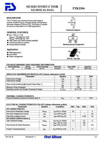
SEMICONDUCTOR FTK2304 TECHNICAL DATA D DESCRIPTION The FTK2304 uses advanced trench technology to G provide excellent RDS(ON), low gate charge and operation with gate voltages as low as 4.5V. This device is suitable for use as a load switch or in PWM applications. S Schematic diagram GENERAL FEATURES D VDS = 30V ,ID = 3.3A 3 RDS(ON) ... See More ⇒
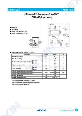
si2304ds.pdf
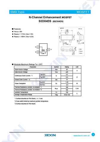
SMD Type MOSFET N-Channel Enhancement MOSFET SI2304DS (KI2304DS) SOT-23 Unit mm Features +0.1 2.9-0.1 +0.1 0.4 -0.1 VDS (V) = 30V 3 RDS(ON) 117m (VGS = 10V) RDS(ON) 190m (VGS = 4.5V) 1 2 +0.1 +0.05 0.95 -0.1 0.1 -0.01 +0.1 1.9 -0.1 G 1 1.Gate 3 D 2.Source S 2 3.Drain Absolute Maximum Ratings Ta = 25 Parameter Symbol Rating Unit ... See More ⇒
si2304ds-3.pdf

SMD Type MOSFET N-Channel Enhancement MOSFET SI2304DS (KI2304DS) SOT-23-3 Unit mm +0.2 2.9 -0.1 +0.1 0.4-0.1 Features 3 VDS (V) = 30V RDS(ON) 117m (VGS = 10V) RDS(ON) 190m (VGS = 4.5V) 1 2 +0.02 +0.1 0.15 -0.02 0.95 -0.1 +0.1 1.9 -0.2 G 1 3 D 1. Gate S 2 2. Source 3. Drain Absolute Maximum Ratings Ta = 25 Parameter Symbol Ratin... See More ⇒
ki2304ds.pdf
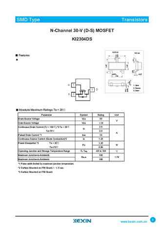
SMD Type Transistors N-Channel 30-V (D-S) MOSFET KI2304DS SOT-23 Unit mm +0.1 2.9-0.1 Features +0.1 0.4-0.1 3 12 +0.1 +0.05 0.95-0.1 0.1-0.01 +0.1 1.9-0.1 1.Base 1. Gate 2.Emitter 2. Source 3. Drain 3.collector Absolute Maximum Ratings Ta = 25 Parameter Symbol Rating Unit Drain-Source Voltage VDS 30 V Gate-Source Voltage VGS 20 Continuous Drain Current (TJ = 150 ) *... See More ⇒
si2304ds ki2304ds.pdf
SMD Type MOSFET N-Channel Enhancement MOSFET SI2304DS (KI2304DS) SOT-23-3 Unit mm +0.2 2.9 -0.1 +0.1 0.4-0.1 Features 3 VDS (V) = 30V RDS(ON) 117m (VGS = 10V) RDS(ON) 190m (VGS = 4.5V) 1 2 +0.02 +0.1 0.15 -0.02 0.95 -0.1 +0.1 1.9 -0.2 G 1 3 D 1. Gate S 2 2. Source 3. Drain Absolute Maximum Ratings Ta = 25 Parameter Symbol Ratin... See More ⇒
am2304.pdf
AiT Semiconductor Inc. AM2304 www.ait-ic.com MOSFET N-CHANNEL ENHANCEMENT MODE MOSFET DESCRIPTION FEATURES AM2304 is available in a SOT-23 package. 30V/5.1A R = 25m (max.) @ V = 10V DS(ON) GS R = 35m (max.) @ V = 4.5V DS(ON) GS Reliable and Rugged Available in a SOT-23 package. ORDERING INFORMATION APPLICATION Power Management in Notebook Computer, Por... See More ⇒
chm2304gp.pdf
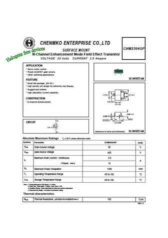
CHENMKO ENTERPRISE CO.,LTD CHM2304GP SURFACE MOUNT N-Channel Enhancement Mode Field Effect Transistor VOLTAGE 30 Volts CURRENT 2.8 Ampere APPLICATION * Servo motor control. * Power MOSFET gate drivers. * Other switching applications. SC-59/SOT-346 FEATURE * Small flat package. (SC-59 ) * High density cell design for extremely low RDS(ON). * Rugged and reliable. (2) * High sat... See More ⇒
ctn2304.pdf
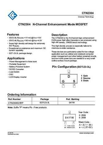
CTN2304 Crownpo Technology CTN2304 N-Channel Enhancement Mode MOSFET Features Description 30V/2.5A,RDS(ON)=117m @VGS=10V The CTN2304 is the N-Channel logic enhancement 20V/2.4A,R =190 m @VGS=4.5V mode power field effect transistors are produced using DS(ON) high cell density , DMOS trench technology. Super high density cell design for extremely low RDS(ON) Exc... See More ⇒
gsm2304a.pdf
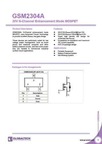
GSM2304A 30V N-Channel Enhancement Mode MOSFET Product Description Features GSM2304A, N-Channel enhancement mode 30V/2.6A,RDS(ON)=82m @VGS=10V MOSFET, uses Advanced Trench Technology 30V/2.0A,RDS(ON)=108m @VGS=4.5V to provide excellent RDS(ON), low gate charge. Super high density cell design for extremely low RDS (ON) These devices are particularly suited for low Exce... See More ⇒
gsm2304.pdf
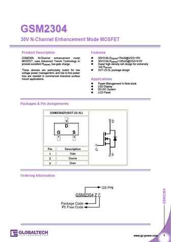
GSM2304 GSM2304 30V N-Channel Enhancement Mode MOSFET Product Description Features GSM2304, N-Channel enhancement mode 30V/3.6A,RDS(ON)=78m @VGS=10V MOSFET, uses Advanced Trench Technology to 30V/2.8A,RDS(ON)=105m @VGS=4.5V provide excellent RDS(ON), low gate charge. Super high density cell design for extremely low RDS (ON) These devices are particularly suited for low ... See More ⇒
gsm2304as.pdf
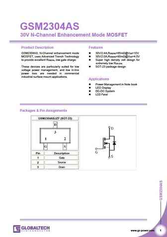
GSM2304AS 30V N-Channel Enhancement Mode MOSFET Product Description Features GSM2304AS, N-Channel enhancement mode 30V/2.4A,RDS(ON)=65m @VGS=10V MOSFET, uses Advanced Trench Technology 30V/2.0A,RDS(ON)=90m @VGS=4.5V to provide excellent RDS(ON), low gate charge. Super high density cell design for extremely low RDS (ON) These devices are particularly suited for low SOT-2... See More ⇒
gsm2304s.pdf
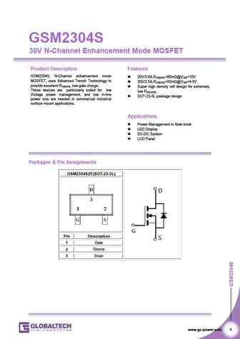
GSM2304S 30V N-Channel Enhancement Mode MOSFET Product Description Features GSM2304S, N-Channel enhancement mode 30V/3.6A,RDS(ON)=60m @VGS=10V MOSFET, uses Advanced Trench Technology to 30V/2.5A,RDS(ON)=85m @VGS=4.5V provide excellent RDS(ON) ,low gate charge. Super high density cell design for extremely These devices are particularly suited for low low RDS (O... See More ⇒
nce2304.pdf
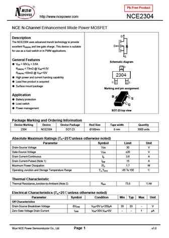
Pb Free Product http //www.ncepower.com NCE2304 NCE N-Channel Enhancement Mode Power MOSFET D Description The NCE2304 uses advanced trench technology to provide G excellent RDS(ON) and low gate charge .This device is suitable for use as a load switch or in PWM applications. S General Features Schematic diagram VDS = 30V,ID = 3.6A RDS(ON) ... See More ⇒
shd230409.pdf
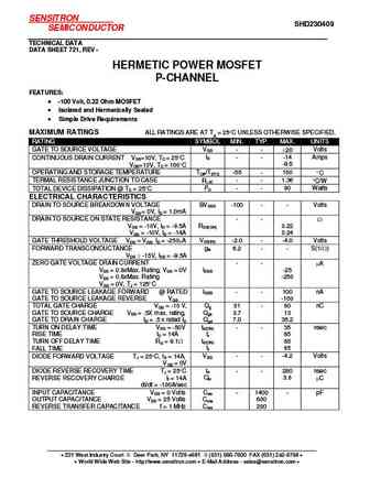
SENSITRON SHD230409 SEMICONDUCTOR TECHNICAL DATA DATA SHEET 721, REV - HERMETIC POWER MOSFET P-CHANNEL FEATURES -100 Volt, 0.22 Ohm MOSFET Isolated and Hermetically Sealed Simple Drive Requirements MAXIMUM RATINGS ALL RATINGS ARE AT TA = 25 C UNLESS OTHERWISE SPECIFIED. RATING SYMBOL MIN. TYP. MAX. UNITS GATE TO SOURCE VOLTAGE VGS - - 20 Volts ID - - -14 Amps CON... See More ⇒
shd230452.pdf
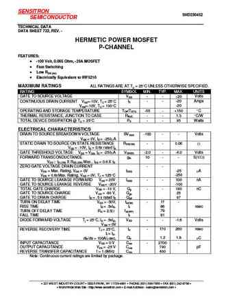
SENSITRON SHD230452 SEMICONDUCTOR TECHNICAL DATA DATA SHEET 722, REV. - HERMETIC POWER MOSFET P-CHANNEL FEATURES -100 Volt, 0.065 Ohm, -20A MOSFET Fast Switching Low RDS (on) Electrically Equivalent to IRF5210 MAXIMUM RATINGS ALL RATINGS ARE AT TC = 25 C UNLESS OTHERWISE SPECIFIED. RATING SYMBOL MIN. TYP. MAX. UNITS GATE TO SOURCE VOLTAGE VGS - - 20 Volts ID -... See More ⇒
shd230405.pdf
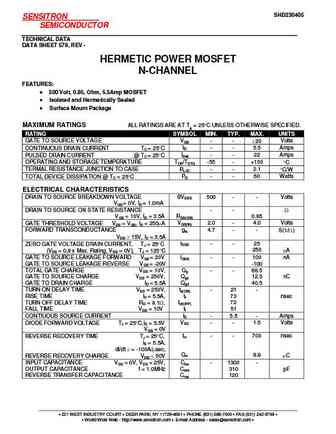
SHD230405 SENSITRON SEMICONDUCTOR TECHNICAL DATA DATA SHEET 579, REV - HERMETIC POWER MOSFET N-CHANNEL FEATURES 500 Volt, 0.85, Ohm, 5.5Amp MOSFET Isolated and Hermetically Sealed Surface Mount Package MAXIMUM RATINGS ALL RATINGS ARE AT TA = 25 C UNLESS OTHERWISE SPECIFIED. RATING SYMBOL MIN. TYP. MAX. UNITS GATE TO SOURCE VOLTAGE VGS - - 20 Volts ID - - 5.5 Amps ... See More ⇒
ssm2304agn.pdf
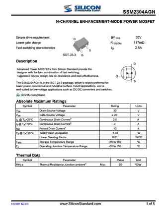
SSM2304AGN N-CHANNEL ENHANCEMENT-MODE POWER MOSFET Simple drive requirement BV 30V DSS D Lower gate charge R 117m DS(ON) Fast switching characteristics ID 2.5A S SOT-23-3 G Description D Advanced Power MOSFETs from Silicon Standard provide the designer with the best combination of fast switching, ruggedized device design, low on-resistance and cost-effectiveness. G S The SS... See More ⇒
ssm2304gn.pdf
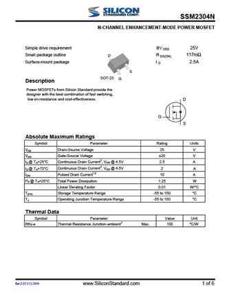
SSM2304N N-CHANNEL ENHANCEMENT-MODE POWER MOSFET Simple drive requirement BV 25V DSS Small package outline R 117m D DS(ON) Surface-mount package I 2.5A D S SOT-23 G Description Power MOSFETs from Silicon Standard provide the designer with the best combination of fast switching, low on-resistance and cost-effectiveness. D G S Absolute Maximum Ratings Symbol Parameter Rati... See More ⇒
sl2304.pdf
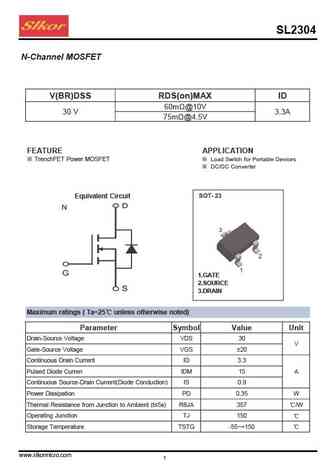
SL2304 N-Channel MOSFET V(BR)DSS RDS(on)MAX ID 60m @10V 30 V 3.3A 75m @4.5V FEATURE APPLICATION TrenchFET Power MOSFET Load Switch for Portable Devices DC/DC Converter Equivalent Circuit 1.GATE 2.SOURCE 3.DRAIN Maximum ratings ( Ta=25 unless otherwise noted) Parameter Symbol Value Unit Drain-Source Voltage VDS 30 V Gate-Source Voltage VGS 20 Continuous Drain... See More ⇒
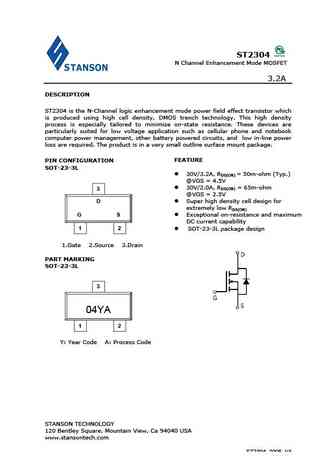
st2304srg.pdf

ST2304SRG N Channel Enhancement Mode MOSFET 3.2A DESCRIPTION ST2304SRG is the N-Channel logic enhancement mode power field effect transistor which is produced using high cell density, DMOS trench technology. This high density process is especially tailored to minimize on-state resistance. These devices are particularly suited for low voltage application such as cellular phone an... See More ⇒
st2304.pdf
ST2304 N Channel Enhancement Mode MOSFET 3.2A DESCRIPTION ST2304 is the N-Channel logic enhancement mode power field effect transistor which is produced using high cell density, DMOS trench technology. This high density process is especially tailored to minimize on-state resistance. These devices are particularly suited for low voltage application such as cellular phone and note... See More ⇒
si2304a.pdf
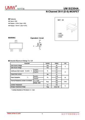
R UMW UM SI2304A N-Channel 30-V (D-S) MOSFET Features SOT 23 VDS (V) = 30V RDS(ON) 57m (VGS =-10V) RDS(ON) 94 m (VGS =-4.5V) 1. GATE 2. SOURCE 3. DRAIN MARKING Equivalent Circuit D G S Absolute Maximum Ratings Ta = 25 Parameter Symbol Rating Unit Drain-Source Voltage VDS 30 V Gate-Source Voltage VGS 20 Ta=25 3.5 Continuous Dr... See More ⇒
as2304.pdf
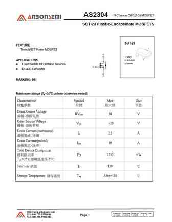
N-Channel 30V(D-S) MOSFET AS2304 SOT-23 Plastic-Encapsulate MOSFETS Dimensions In Millimeters Dimensions In Inches Symbol Min Max Min Max A 0.900 1.150 0.035 0.045 A1 0.000 0.100 0.000 0.004 A2 0.900 1.050 0.035 0.041 b 0.300 0.500 0.012 0.020 c 0.080 0.150 0.003 0.006 D 2.800 3.000 0.110 0.118 E 1.200 1.400 0.047 0.055 E1 2.250 2.550 0.089 0... See More ⇒
si2304.pdf
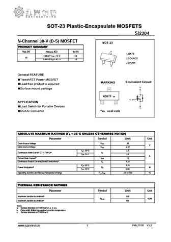
SOT-23 Plastic-Encapsulate MOSFETS SI2304 N-Channel 30-V (D-S) MOSFET SOT-23 PRODUCT SUMMARY VDS (V) rDS(on) (W) ID (A) 3 1.GATE 0.055 @ V 2.5 GS = 10 V 30 30 2.SOURCE 0.080 @ VGS = 4.5 V 2.0 3.DRAIN 1 2 General FEATURE TrenchFET Power MOSFET Equivalent Circuit MARKING Lead free product is acquired Surface mount package A69TF w APPLICATION Load Switch for Por... See More ⇒
wst2304.pdf
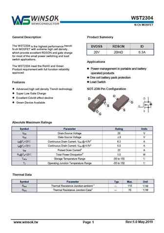
WST2304 N-Ch MOSFET General Description Product Summery The WST2304 is the highest performance trench BVDSS RDSON ID N-ch MOSFET with extreme high cell density , 20V 20m 6.3A which provide excellent RDSON and gate charge for most of the small power switching and load switch applications. Applications The WST2304 meet the RoHS and Green Power management in portable and ... See More ⇒
wst2304a.pdf
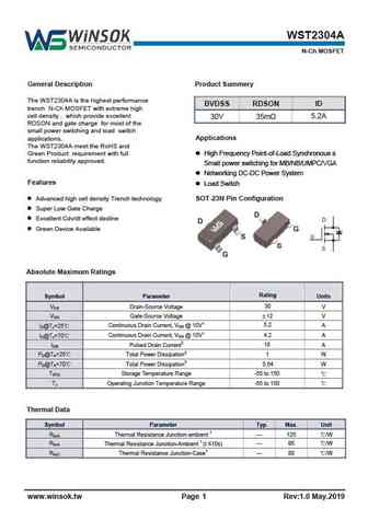
WST2304A N-Ch MOSFET General Description Product Summery The WST2304A is the highest performance BVDSS RDSON ID trench N-Ch MOSFET with extreme high cell density , which provide excellent 30V 35m 5.2A RDSON and gate charge for most of the small power switching and load switch Applications applications. The WST2304A meet the RoHS and Green Product requirement with full ... See More ⇒
ap2304gn.pdf
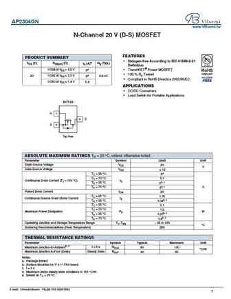
AP2304GN www.VBsemi.tw N-Channel 20 V (D-S) MOSFET FEATURES PRODUCT SUMMARY Halogen-free According to IEC 61249-2-21 VDS (V) RDS(on) ( ) ID (A)e Qg (Typ.) Definition 0.028 at VGS = 4.5 V TrenchFET Power MOSFET 6a 100 % Rg Tested 20 0.042 at VGS = 2.5 V 6a 8.8 nC Compliant to RoHS Directive 2002/95/EC 0.050 at VGS = 1.8 V 5.6 APPLICATIONS DC/DC Conve... See More ⇒
st2304.pdf
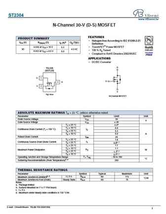
ST2304 www.VBsemi.tw N-Channel 30-V (D-S) MOSFET FEATURES PRODUCT SUMMARY Halogen-free According to IEC 61249-2-21 VDS (V) RDS(on) ( ) ID (A)a Qg (Typ.) Definition 0.030 at VGS = 10 V TrenchFET Power MOSFET 6.5 30 4.5 nC 100 % Rg Tested 0.033 at VGS = 4.5 V 6.0 Compliant to RoHS Directive 2002/95/EC APPLICATIONS DC/DC Converter D TO-236 (SOT-23) G 1... See More ⇒
yjl2304a.pdf
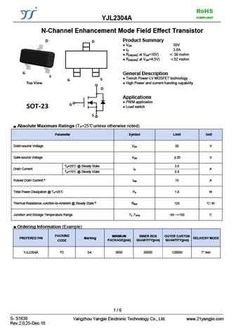
RoHS COMPLIANT YJL2304A N-Channel Enhancement Mode Field Effect Transistor Product Summary V 30V DS I 3.6A D R ( at V =10V) 39 mohm DS(ON) GS R ( at V =4.5V) 52 mohm DS(ON) GS General Description Trench Power LV MOSFET technology High Power and current handing capability Applications PWM application Load switch Absolute M... See More ⇒
2sc2304.pdf
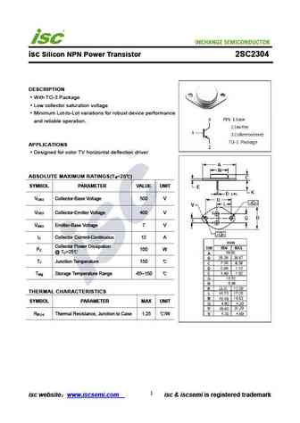
INCHANGE Semiconductor isc Silicon NPN Power Transistor 2SC2304 DESCRIPTION With TO-3 Package Low collector saturation voltage Minimum Lot-to-Lot variations for robust device performance and reliable operation. APPLICATIONS Designed for color TV horizontal deflection driver ABSOLUTE MAXIMUM RATINGS(T =25 ) a SYMBOL PARAMETER VALUE UNIT V Collector-Base Voltage 500 V CBO ... See More ⇒
Detailed specifications: 2N6798U, 2N6800LCC4, 2N6800U, 2N6802U, 2N6845LCC4, 2N6845U, 2N6847U, 2303, AON7506, 2305, 4414, 4614, 4800, 8958, 9926, 045Y, 06N03
Keywords - 2304 MOSFET specs
2304 cross reference
2304 equivalent finder
2304 pdf lookup
2304 substitution
2304 replacement
Need a MOSFET replacement? Our guide shows you how to find a perfect substitute by comparing key parameters and specs
History: IRFB3207
🌐 : EN ES РУ

LIST
Last Update
MOSFET: AUB034N10 | AUB033N08BG | AUB026N085 | AUA062N08BG | AUA060N08AG | AUA056N08BGL | AUA039N10 | ASW80R290E | ASW65R120EFD | ASW65R110E
Popular searches
2n3904 | bc547 datasheet | k3797 mosfet | bs170 datasheet | tip41c | irfp460 | irfz44n mosfet | lm317t datasheet