4414 Specs and Replacement
Type Designator: 4414
Type of Transistor: MOSFET
Type of Control Channel: N-Channel
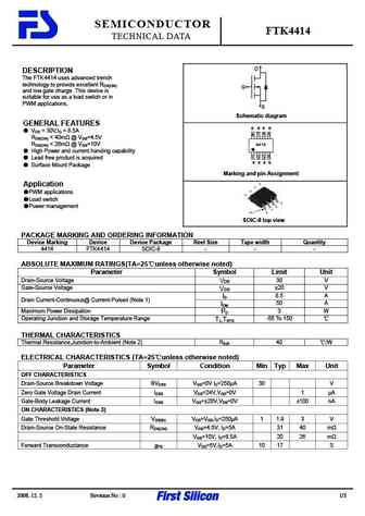
Absolute Maximum Ratings
Pd ⓘ - Maximum Power Dissipation: 3 W
|Vds|ⓘ - Maximum Drain-Source Voltage: 30 V
|Vgs|ⓘ - Maximum Gate-Source Voltage: 20 V
|Id| ⓘ - Maximum Drain Current: 8.5 A
Tj ⓘ - Maximum Junction Temperature: 150 °C
Electrical Characteristics
tr ⓘ - Rise Time: 4.2 nS
Cossⓘ - Output Capacitance: 102 pF
RDSonⓘ - Maximum Drain-Source On-State Resistance: 0.026 Ohm
Package: SOIC-8
4414 substitution
- MOSFET ⓘ Cross-Reference Search
4414 datasheet
4414.pdf
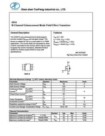
Shen zhen TuoFeng industrial co., LTD 4414 N-Channel Enhancement Mode Field Effect Transistor General Description Features The AO4414 uses advanced trench technology to VDS (V) = 30V provide excellent RDS(ON) and low gate charge. This ID = 8.5A (VGS = 10V) device is suitable for use as a load switch or in PWM RDS(ON) ... See More ⇒
2sa1683 2sc4414.pdf
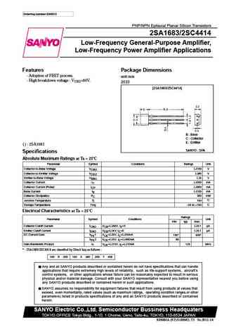
Ordering number EN3012 PNP/NPN Epitaxial Planar Silicon Transistors 2SA1683/2SC4414 Low-Frequency General-Purpose Amplifier, Low-Frequency Power Amplifier Applications Features Package Dimensions Adoption of FBET process. unit mm High breakdown voltage VCEO>80V. 2033 [2SA1683/2SC4414] B Base C Collector E Emitter ( ) 2SA1683 SANYO SPA Specifications Absolute... See More ⇒
ut4414.pdf
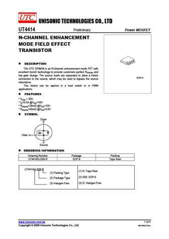
UNISONIC TECHNOLOGIES CO., LTD UT4414 Preliminary Power MOSFET N-CHANNEL ENHANCEMENT MODE FIELD EFFECT TRANSISTOR DESCRIPTION The UTC UT4414 is an N-channel enhancement mode FET with excellent trench technology to provide customers perfect RDS(ON) and low gate charge. The source leads are separated to allow a Kelvin SOP-8 connection to the source, which may be used to bypas... See More ⇒
ssf4414.pdf
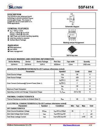
SSF4414 D DESCRIPTION The SSF4414 uses advanced trench technology to provide excellent RDS(ON) G and low gate charge .This device is suitable for use as a load switch or in PWM applications. S Schematic diagram GENERAL FEATURES V = 30V,I = 8.5A DS D R ... See More ⇒
Detailed specifications: 2N6800U, 2N6802U, 2N6845LCC4, 2N6845U, 2N6847U, 2303, 2304, 2305, IRFP450, 4614, 4800, 8958, 9926, 045Y, 06N03, 10N60A, 10N60AF
Keywords - 4414 MOSFET specs
4414 cross reference
4414 equivalent finder
4414 pdf lookup
4414 substitution
4414 replacement
Step-by-step guide to finding a MOSFET replacement. Cross-reference parts and ensure compatibility for your repair or project.
🌐 : EN ES РУ

LIST
Last Update
MOSFET: AUB034N10 | AUB033N08BG | AUB026N085 | AUA062N08BG | AUA060N08AG | AUA056N08BGL | AUA039N10 | ASW80R290E | ASW65R120EFD | ASW65R110E
Popular searches
k3797 mosfet | bs170 datasheet | tip41c | irfp460 | irfz44n mosfet | lm317t datasheet | irf540 | bc337