9926 Specs and Replacement
Type Designator: 9926
Type of Transistor: MOSFET
Type of Control Channel: N-Channel
Absolute Maximum Ratings
Pd ⓘ - Maximum Power Dissipation: 1.25 W
|Vds|ⓘ - Maximum Drain-Source Voltage: 20 V
|Vgs|ⓘ - Maximum Gate-Source Voltage: 10 V
|Id| ⓘ - Maximum Drain Current: 6 A
Tj ⓘ - Maximum Junction Temperature: 150 °C
Electrical Characteristics
tr ⓘ - Rise Time: 9 nS
Cossⓘ - Output Capacitance: 140 pF
RDSonⓘ - Maximum Drain-Source On-State Resistance: 0.03 Ohm
Package: SOP-8
9926 substitution
- MOSFET ⓘ Cross-Reference Search
9926 datasheet
9926.pdf
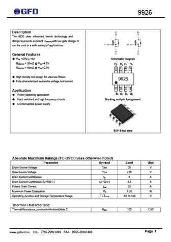
9926 Description The 9926 uses advanced trench technology and design to provide excellent RDS(ON) with low gate charge. It can be used in a wide variety of applications. General Features VDS =20V,ID =6A Schematic diagram RDS(ON) ... See More ⇒
fds9926a.pdf
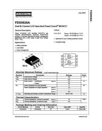
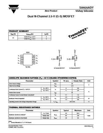
July 2003 FDS9926A Dual N-Channel 2.5V Specified PowerTrench MOSFET Features General Description These N-Channel 2.5V specified MOSFETs use 6.5 A, 20 V. RDS(ON) = 30 m @ VGS = 4.5 V Fairchild Semiconductor s advanced PowerTrench RDS(ON) = 43 m @ VGS = 2.5 V. process. It has been optimized for power management applications with a wide range of gate drive voltage Optimized ... See More ⇒

dmg9926usd.pdf
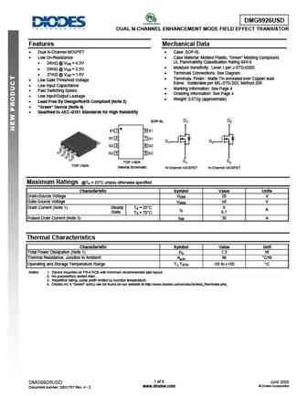
DMG9926USD DUAL N-CHANNEL ENHANCEMENT MODE FIELD EFFECT TRANSISTOR Features Mechanical Data Dual N-Channel MOSFET Case SOP-8L Low On-Resistance Case Material Molded Plastic, Green Molding Compound. UL Flammability Classification Rating 94V-0 24m @ VGS = 4.5V Moisture Sensitivity Level 1 per J-STD-020D 29m @ VGS = 2.5V Terminals Conn... See More ⇒
dmg9926udm.pdf
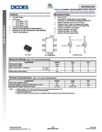
DMG9926UDM DUAL N-CHANNEL ENHANCEMENT MODE MOSFET Please click here to visit our online spice models database. Features Mechanical Data Low Gate Charge Case SOT-26 Low RDS(ON) Case Material - Molded Plastic, Green Molding Compound. UL Flammability Classification Rating 94V-0 28m @VGS = 4.5V Moisture Sensitivity Level 1 per J-STD-020D 32m @... See More ⇒
ud9926.pdf
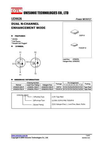
UNISONIC TECHNOLOGIES CO., LTD UD9926 Power MOSFET DUAL N-CHANNEL ENHANCEMENT MODE SOP-8 FEATURES * 20V/6A * Low RDS(ON) * Reliable and Rugged SYMBOL TSSOP-8 Lead-free UD9926L Halogen-free UD9926G ORDERING INFORMATION Ordering Number Pin Assignment Package Packing Normal Lead Free Plating Halogen Free 1 2 3 4 5 6 7 8 UD9926-S08-R UD9926L-S08-R UD9926G-S08-R... See More ⇒
tsm9926dcs.pdf
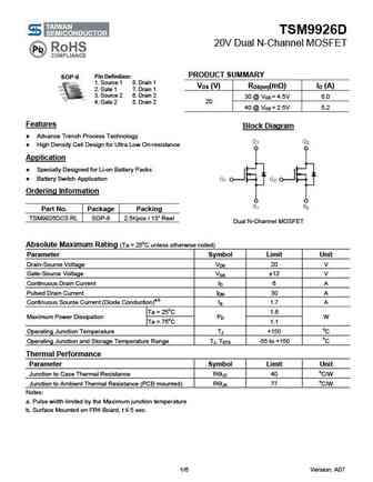
TSM9926D 20V Dual N-Channel MOSFET PRODUCT SUMMARY SOP-8 Pin Definition 1. Source 1 8. Drain 1 VDS (V) RDS(on)(m ) ID (A) 2. Gate 1 7. Drain 1 3. Source 2 6. Drain 2 30 @ VGS = 4.5V 6.0 4. Gate 2 5. Drain 2 20 40 @ VGS = 2.5V 5.2 Features Block Diagram Advance Trench Process Technology High Density Cell Design for Ultra Low On-resistance Application ... See More ⇒
cjq9926.pdf
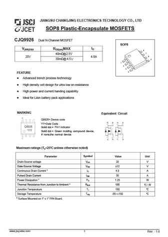
JIANGSU CHANGJING ELECTRONICS TECHNOLOGY CO., LTD CJQ9926 Dual N-Channel MOSFET SOP8 ID V(BR)DSS RDS(on)MAX 40m @2.5V 20V 4.8A 30m @ 4.5 V FEATURE Advanced trench process technology High density cell design for ultra low on-resistance High power and current handing capability Ideal for Liion battery pack applications MARK... See More ⇒
pt9926.pdf
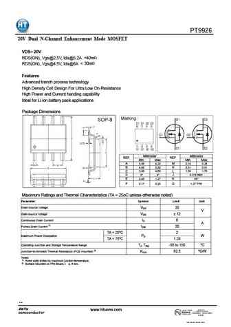
PT9926 20V Dual N-Channel Enhancement Mode MOSFET VDS= 20V RDS(ON), Vgs@2.5V, Ids@5.2A ... See More ⇒
cem9926a.pdf
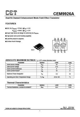
CEM9926A Dual N-Channel Enhancement Mode Field Effect Transistor FEATURES 20V, 6A, RDS(ON) = 27m @VGS = 4.5V. RDS(ON) = 40m @VGS = 2.5V. Super high dense cell design for extremely low RDS(ON). High power and current handing capability. D1 D1 D2 D2 Lead free product is acquired. 8 7 6 5 Surface mount Package. SO-8 1 2 3 4 1 S1 G1 S2 G2 ABSOLUTE MAXIMUM RATINGS TA = 25 C unl... See More ⇒
h9926s.pdf
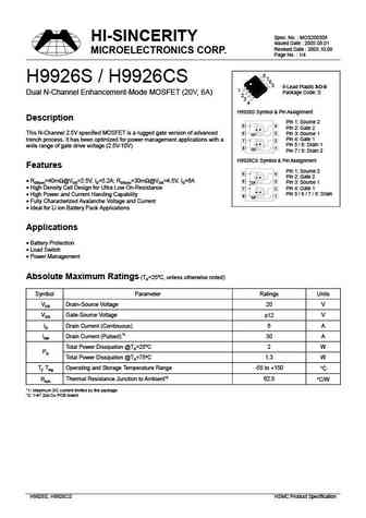
Spec. No. MOS200508 HI-SINCERITY Issued Date 2005.08.01 Revised Date 2005.10.06 MICROELECTRONICS CORP. Page No. 1/4 8 76 H9926S / H9926CS 5 8-Lead Plastic SO-8 1 Package Code S Dual N-Channel Enhancement-Mode MOSFET (20V, 6A) 2 3 4 H9926S Symbol & Pin Assignment Description Pin 1 Source 2 5 4 Pin 2 Gate 2 6 3 This N-Channel 2.5V specified MOSFET is a rugge... See More ⇒
h9926ts.pdf
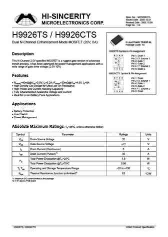
Spec. No. MOS200513 HI-SINCERITY Issued Date 2005.10.01 Revised Date 2005.10.06 MICROELECTRONICS CORP. Page No. 1/4 H9926TS / H9926CTS 8-Lead Plastic TSSOP-8L Dual N-Channel Enhancement-Mode MOSFET (20V, 6A) Package Code TS H9926TS Symbol & Pin Assignment Description 8 7 6 5 Pin 1 Drain 1 Q2 Pin 2 / 3 Source 1 This N-Channel 2.5V specified MOSFET is a rugged gate versi... See More ⇒
ao9926c.pdf
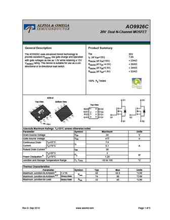
AO9926C 20V Dual N-Channel MOSFET General Description Product Summary VDS The AO9926C uses advanced trench technology to 20V 7.6A provide excellent RDS(ON), low gate charge and operation ID (at VGS=10V) with gate voltages as low as 1.8V while retaining a 12V ... See More ⇒
ao9926b.pdf
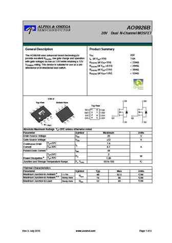
AO9926B 20V Dual N-Channel MOSFET General Description Product Summary VDS 20V The AO9926B uses advanced trench technology to provide excellent RDS(ON), low gate charge and operation ID (at VGS=10V) 7.6A with gate voltages as low as 1.8V while retaining a 12V RDS(ON) (at VGS=10V) ... See More ⇒
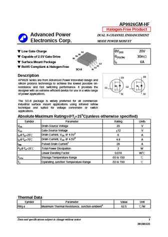
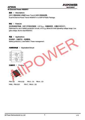
ap9926gm-hf.pdf
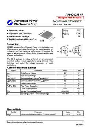
AP9926GM-HF Halogen-Free Product Advanced Power Dual N-CHANNEL ENHANCEMENT Electronics Corp. MODE POWER MOSFET Low Gate Charge BVDSS 20V D2 D2 D1 Capable of 2.5V Gate Drive RDS(ON) 30m D1 Surface Mount Package ID 6A G2 S2 RoHS Compliant & Halogen-Free G1 S1 SO-8 Description D2 D1 AP9926 series are from Advanced Power innovated design and silicon process te... See More ⇒
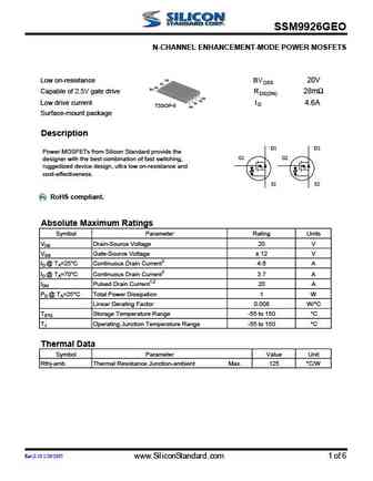
ap9926go.pdf
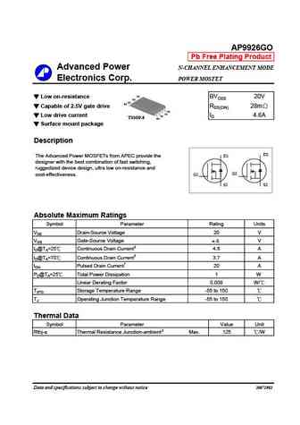
AP9926GO Pb Free Plating Product Advanced Power N-CHANNEL ENHANCEMENT MODE Electronics Corp. POWER MOSFET G2 Low on-resistance BVDSS 20V S2 S2 D2 Capable of 2.5V gate drive RDS(ON) 28m G1 S1 Low drive current S1 ID 4.6A TSSOP-8 D1 Surface mount package Description D2 The Advanced Power MOSFETs fr... See More ⇒
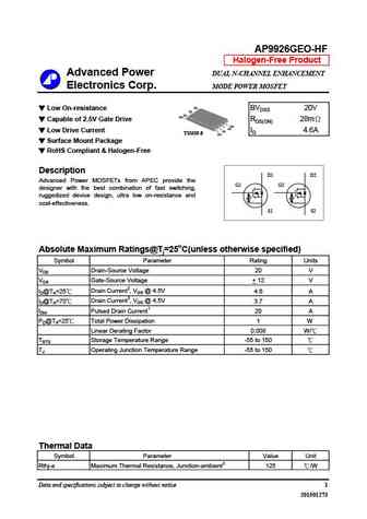
ap9926geo-hf.pdf
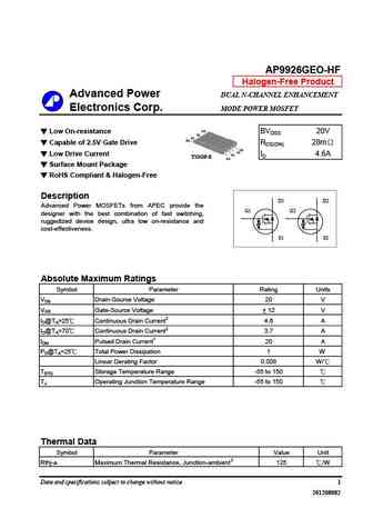
AP9926GEO-HF Halogen-Free Product Advanced Power DUAL N-CHANNEL ENHANCEMENT Electronics Corp. MODE POWER MOSFET G2 Low On-resistance BVDSS 20V S2 S2 D2 Capable of 2.5V Gate Drive RDS(ON) 28m G1 S1 Low Drive Current S1 ID 4.6A TSSOP-8 D1 Surface Mount Package RoHS Compliant & Halogen-Free Description D1 D2 Advanced Power MOSFETs from APEC provide the G1 ... See More ⇒
ap9926gm.pdf
AP9926GM-HF Halogen-Free Product Advanced Power DUAL N-CHANNEL ENHANCEMENT Electronics Corp. MODE POWER MOSFET Low Gate Charge BVDSS 20V D2 D2 D1 Capable of 2.5V Gate Drive RDS(ON) 30m D1 Surface Mount Package ID 6A G2 S2 RoHS Compliant & Halogen-Free G1 S1 SO-8 Description D2 D1 AP9926 series ar... See More ⇒
ap9926gem.pdf
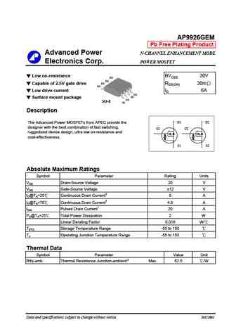
AP9926GEM Pb Free Plating Product Advanced Power N-CHANNEL ENHANCEMENT MODE Electronics Corp. POWER MOSFET Low on-resistance BVDSS 20V D2 D2 Capable of 2.5V gate drive D1 RDS(ON) 30m D1 Low drive current ID 6A G2 S2 Surface mount package G1 SO-8 S1 Description The Advanced Power MOSFETs from APEC provide the D1 D2 designer with the best combination of fast sw... See More ⇒
ap9926geo.pdf
AP9926GEO-HF Halogen-Free Product Advanced Power DUAL N-CHANNEL ENHANCEMENT Electronics Corp. MODE POWER MOSFET G2 Low On-resistance BVDSS 20V S2 S2 D2 Capable of 2.5V Gate Drive RDS(ON) 28m G1 S1 Low Drive Current S1 ID 4.6A TSSOP-8 D1 Surface Mount Package RoHS Compliant & Halogen-Free Description D1 D2 Advanced Power MOSFETs from APEC provide the G1 ... See More ⇒
am9926n.pdf
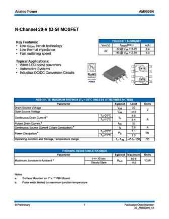
Analog Power AM9926N N-Channel 20-V (D-S) MOSFET PRODUCT SUMMARY Key Features rDS(on) (m ) VDS (V) ID(A) Low r trench technology DS(on) 30 @ VGS = 4.5V 6.9 Low thermal impedance 20 40 @ VGS = 2.5V 6.0 Fast switching speed Typical Applications White LED boost converters Automotive Systems Industrial DC/DC Conversion Circuits ABSOLUTE MAXIMUM ... See More ⇒
9926b.pdf
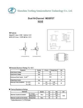
Shenzhen Tuofeng Semiconductor Technology Co., Ltd SMD Type MOSFET Dual N-Channel MOSFET 9926B Features 6.5A, 20 V . rDS(on) = 0. 022 @VGS =4.5 V 5.5A , 20 V rDS(on) = 0. 035 @VGS =2.5 V. Absolute Maximum Ratings Ta = 25 Parameter Symbol 10 secs Steady Sate Unit Drai n-S ourc e V ol t age V DS 20 V Gat e-S ourc e V ol t age V GS 10 V 6.5 A Continuous Drain Current Ta=25 ID Pulsed ... See More ⇒
9926a.pdf

Shenzhen Tuofeng Semiconductor Technology Co., Ltd SMD Type MOSFET Dual N-Channel MOSFET 9926A Features 6A , 20 V . rDS(on) = 0. 030 @VGS =4.5 V 5.2A , 20 V rDS(on) = 0. 040 @VGS =2.5 V. Absolute Maximum Ratings Ta = 25 Parameter Symbol 10 secs Steady Sate Unit Drai n-S ourc e V ol t age V DS 20 V Gat e-S ourc e V ol t age V GS 10 V Continuous Drain Current Ta=25 6 A ID Pulsed Dra... See More ⇒
mtdn9926q8.pdf
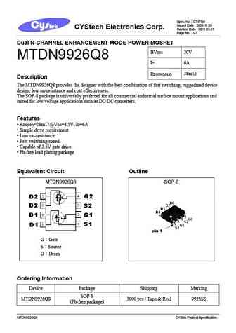
Spec. No. C747Q8 Issued Date 2009.11.09 CYStech Electronics Corp. Revised Date 2011.03.21 Page No. 1/7 Dual N-CHANNEL ENHANCEMENT MODE POWER MOSFET BVDSS 20V MTDN9926Q8 ID 6A 28m RDSON(MAX) Description The MTDN9926Q8 provides the designer with the best combination of fast switching, ruggedized device design, low on-resistance and cost effectiveness. The SOP-8... See More ⇒
apm9926c.pdf
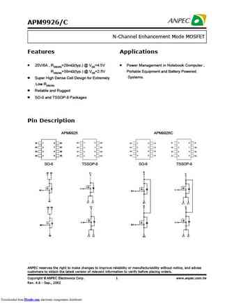
APM9926/C N-Channel Enhancement Mode MOSFET Features Applications 20V/6A , RDS(ON)=28m (typ.) @ VGS=4.5V Power Management in Notebook Computer , RDS(ON)=38m (typ.) @ VGS=2.5V Portable Equipment and Battery Powered Systems. Super High Dense Cell Design for Extremely Low RDS(ON) Reliable and Rugged SO-8 and TSSOP-8 Packages ... See More ⇒
apm9926ak.pdf
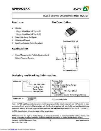
APM9926AK Dual N-Channel Enhancement Mode MOSFET Features Pin Description 20V/6A, RDS(ON) =28m (typ.) @ VGS =4.5V RDS(ON) =34m (typ.) @ VGS =2.5V Super High Dense Cell Design Reliable and Rugged Top View of SOP - 8 Lead Free Available (RoHS Compliant) (8) (7) (6) (5) D1 D1 D2 D2 Applications Power Management in Portable Equipment and Battery Powered Systems (2) (4) G1... See More ⇒
apm9926ccg.pdf
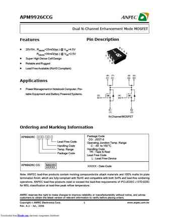
APM9926CCG Dual N-Channel Enhancement Mode MOSFET Features Pin Description 8 20V/5A , RDS(ON)=25m (typ.) @ VGS=4.5V 7 6 5 RDS(ON)=34m (typ.) @ VGS=2.5V 1 2 Super High Dense Cell Design 3 4 Reliable and Rugged Lead Free Available (RoHS Compliant) (8) (7) (6) (5) D1 D1 D2 D2 Applications Power Management in Notebook Computer, Por- table Equipment and Battery Powe... See More ⇒
apm9926k.pdf
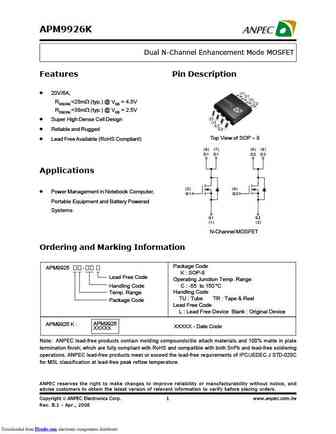
APM9926K Dual N-Channel Enhancement Mode MOSFET Features Pin Description 20V/6A, RDS(ON) =28m (typ.) @ VGS = 4.5V RDS(ON) =38m (typ.) @ VGS = 2.5V Super High Dense Cell Design Reliable and Rugged Top View of SOP - 8 Lead Free Available (RoHS Compliant) (8) (7) (6) (5) D1 D1 D2 D2 Applications (2) (4) Power Management in Notebook Computer, G1 G2 Portable Equipment and ... See More ⇒
apm9926.pdf
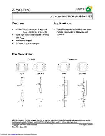
APM9926/C N-Channel Enhancement Mode MOSFET Features Applications 20V/6A , RDS(ON)=28m (typ.) @ VGS=4.5V Power Management in Notebook Computer , RDS(ON)=38m (typ.) @ VGS=2.5V Portable Equipment and Battery Powered Systems. Super High Dense Cell Design for Extremely Low RDS(ON) Reliable and Rugged SO-8 and TSSOP-8 Packages ... See More ⇒
9926b.pdf
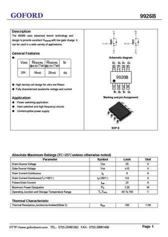
GOFORD 9926B Description The 9926B uses advanced trench technology and design to provide excellent RDS(ON) with low gate charge. It can be used in a wide variety of applications. General Features Schematic diagram VDSS RDS(ON) RDS(ON) ID @4.5V (Typ) @2.5V (Typ) 20V 16m 20 m 6 A B High density cell design for ultra low Rdson Fully characterized avalanche ... See More ⇒
stm9926.pdf
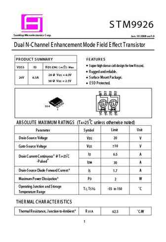
S T M9926 S amHop Microelectronics C orp. J an. 10 2008 ver1.0 Dual N-C hannel E nhancement Mode Field E ffect Transistor P R ODUC T S UMMAR Y F E AT UR E S S uper high dense cell design for low R DS (ON). V DS S ID R DS (ON) ( m W ) Max R ugged and reliable. 28 @ V G S = 4.0V 20V 6.5A S urface Mount Package. 38 @ V G S = 2.5V E S D P rotected. D1 D1 D2 D2 8 7 6 5 S O-8 1 1 2 ... See More ⇒
ssf9926.pdf
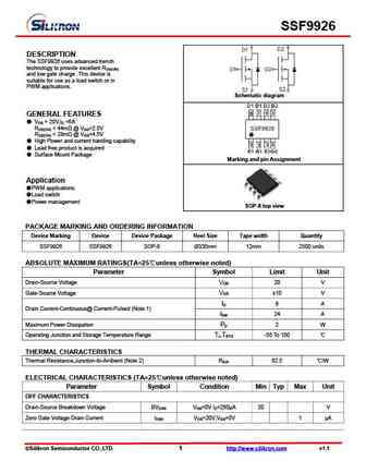
SSF9926 DESCRIPTION The SSF9926 uses advanced trench technology to provide excellent RDS(ON) and low gate charge .This device is suitable for use as a load switch or in PWM applications. Schematic diagram GENERAL FEATURES VDS = 20V,ID =6A R ... See More ⇒
brcs9926sc.pdf
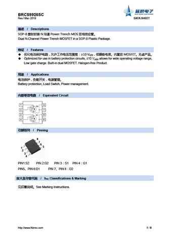
BRCS9926SC Rev.I Mar.-2019 DATA SHEET / Descriptions SOP-8 N Power Trench MOS Dual N-Channel Power Trench MOSFET in a SOP-8 Plastic Package. / Features 10 V MOSFET GSS Optimized for use in battery protecti... See More ⇒
ldn9926et1g.pdf
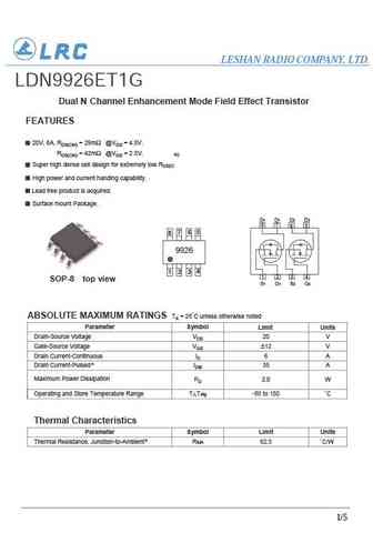
LESHAN RADIO COMPANY, LTD. LDN9926ET1G Dual N Channel Enhancement Mode Field Effect Transistor FEATURES 20V, 6A, RDS(ON) = 29m @VGS = 4.5V. . RDS(ON) = 42m @VGS = 2.5V. N) Super high dense cell design for extremely low RDS(O High power and current handing capability. Lead free product is acquired. Surface mount Package. D1 D1 D2 D2 8 7 6 5 7 6 5 8 9926 4 1 2 3 1 2 3 4 ... See More ⇒
sm9926dsk.pdf
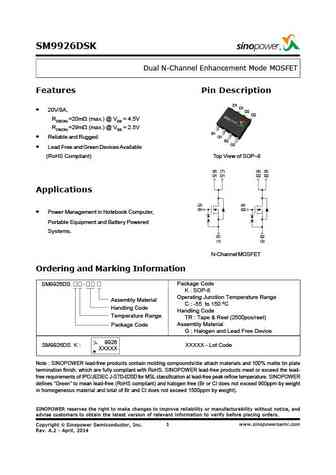
SM9926DSK Dual N-Channel Enhancement Mode MOSFET Features Pin Description D1 D1 20V/8A, D2 D2 RDS(ON) =20m (max.) @ VGS = 4.5V RDS(ON) =29m (max.) @ VGS = 2.5V S1 G1 Reliable and Rugged S2 G2 Lead Free and Green Devices Available (RoHS Compliant) Top View of SOP 8 (8) (7) (6) (5) D1 D1 D2 D2 Applications (2) (4) G1 G2 Power Management in Notebook Computer, Portabl... See More ⇒
ftk9926.pdf
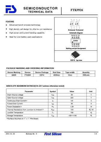
SEMICONDUCTOR FTK9926 TECHNICAL DATA FEATURE Advanced trench process technology High density cell design for ultra low on-resistance N-channel N-channel High power and current handing capability Schematic diagram D 2 D 2 D 1 D 1 Ideal for Liion battery pack applications 6 5 8 7 Q9926 1 2 4 3 S 2 G 2 G 1 S 1 Marking and pin Assignment SOP-8 top view PACKAGE MARKING AN... See More ⇒
si9926dy-hf-s.pdf
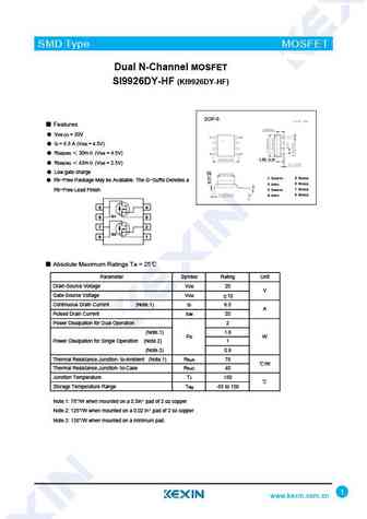
SMD Type MOSFET Dual N-Channel MOSFET SI9926DY-HF (KI9926DY-HF) SOP-8 Features VDS (V) = 20V ID = 6.5 A (VGS = 4.5V) RDS(ON) 30m (VGS = 4.5V) 1.50 0.15 RDS(ON) 43m (VGS = 2.5V) Low gate charge 1 Source 5 Drain Pb-Free Package May be Available. The G-Suffix Denotes a 6 Drain 2 Gate 7 Drain 3 Source Pb-Free Lead Finish 8 Drain 4 Gat... See More ⇒
si9926dy.pdf
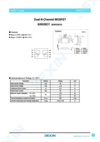
SMD Type MOSFET SMD Type Dual N-Channel MOSFET SI9926DY (KI9926DY) TSSOP-8 Unit mm Features RDS(on) 0.032 @ VGS = 4.5 V 6.45+0.1 -0.1 4.45+0.1 -0.1 RDS(on) 0.045 @ VGS = 2.5 V. 1 Drain1 5 Gate2 2 Source 6 Source2 1 D1 D2 1 3 Source 7 Source2 S1 S2 4 Gate1 8 Drain2 S1 S2 G1 G2 Absolute Maximum Ratings Ta = 25 Parameter ... See More ⇒
si9926dy-s.pdf
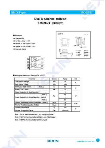
SMD Type MOSFET Dual N-Channel MOSFET SI9926DY (KI9926DY) SOP-8 Features VDS (V) = 20V ID = 6.5 A (VGS = 4.5V) RDS(ON) 30m (VGS = 4.5V) 1.50 0.15 RDS(ON) 43m (VGS = 2.5V) Low gate charge 1 Source 5 Drain 6 Drain 2 Gate 7 Drain 3 Source 8 Drain 4 Gate 5 4 Q1 6 3 7 2 Q2 8 1 Absolute Maximum Ratings Ta = 25 Parameter Symbol R... See More ⇒
si9926bdy.pdf
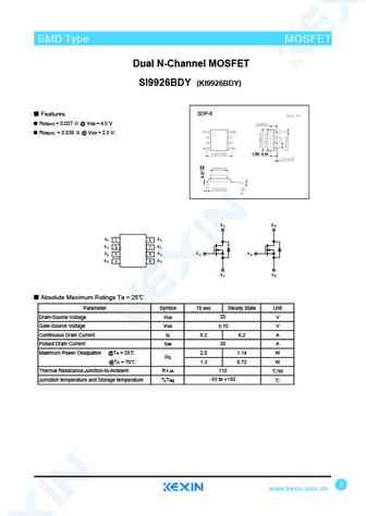
SMD Type MOSFET SMD Type Dual N-Channel MOSFET SI9926BDY (KI9926BDY) Features SOP-8 RDS(on) = 0.027 @ VGS = 4.5 V RDS(on) = 0.036 @ VGS = 2.5 V. 1.50 0.15 D D 1 2 S D 1 1 8 1 G D 1 2 7 1 S D G G 2 3 6 2 1 2 G D 2 4 5 2 S S 1 2 Absolute Maximum Ratings Ta = 25 Parameter Symbol 10 sec Steady State Unit Drain-Source Voltage VDS 20 V Gate-Source Volta... See More ⇒
ki9926a.pdf
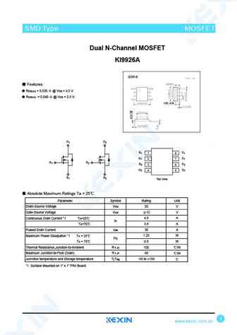
SMD Type MOSFET SMD Type Dual N-Channel MOSFET KI9926A SOP-8 Features RDS(on) = 0.030 @ VGS = 4.5 V RDS(on) = 0.040 @ VGS = 2.5 V. 1.50 0.15 D1 D2 S1 1 D1 8 G1 2 D1 7 G1 G2 S2 3 D2 6 G2 4 D2 5 S1 S2 Top View Absolute Maximum Ratings Ta = 25 Parameter Symbol Rating Unit Drain-Source Voltage VDS 20 V Gate-Source Voltage VGS 12 V Continuous Drain... See More ⇒
am9926.pdf
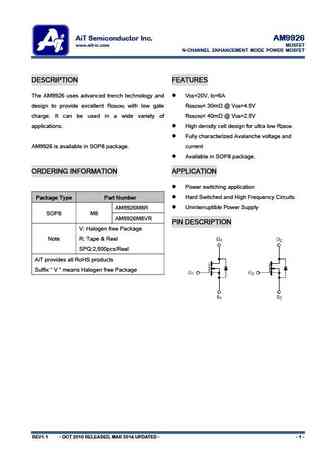
AiT Semiconductor Inc. AM9926 www.ait-ic.com MOSFET N-CHANNEL ENHANCEMENT MODE POWER MOSFET DESCRIPTION FEATURES The AM9926 uses advanced trench technology and V =20V, I =6A DS D design to provide excellent R with low gate R ... See More ⇒
blm9926.pdf
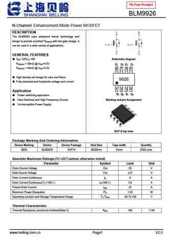
Pb Free Product BLM9926 N-Channel Enhancement Mode Power MOSFET DESCRIPTION The BLM9926 uses advanced trench technology and design to provide excellent RDS(ON) with low gate charge. It can be used in a wide variety of applications. GENERAL FEATURES VDS =20V,ID =6A Schematic diagram RDS(ON) ... See More ⇒
chm9926jgp.pdf
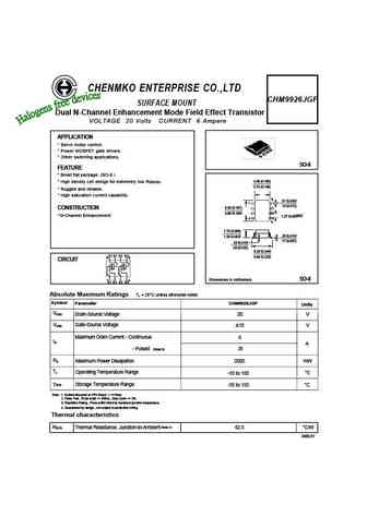
CHENMKO ENTERPRISE CO.,LTD CHM9926JGP SURFACE MOUNT Dual N-Channel Enhancement Mode Field Effect Transistor VOLTAGE 20 Volts CURRENT 6 Ampere APPLICATION * Servo motor control. * Power MOSFET gate drivers. * Other switching applications. SO-8 FEATURE * Small flat package. (SO-8 ) ( ) * High density cell design for extremely low RDS(ON). 4.06 0.160 ( ) 3.70 0.146 * Rugged and ... See More ⇒
chm9926pagp.pdf
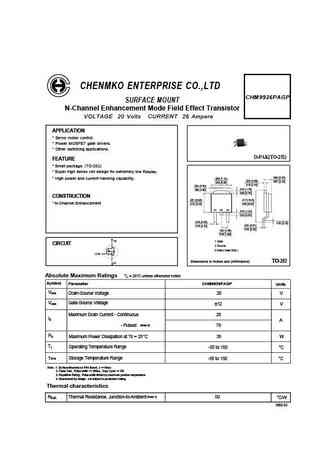
CHENMKO ENTERPRISE CO.,LTD CHM9926PAGP SURFACE MOUNT N-Channel Enhancement Mode Field Effect Transistor VOLTAGE 20 Volts CURRENT 26 Ampere APPLICATION * Servo motor control. * Power MOSFET gate drivers. * Other switching applications. D-PAK(TO-252) FEATURE * Small package. (TO-252) * Super high dense cell design for extremely low RDS(ON). .094 (2.40) .280 (7.10) * High power ... See More ⇒
chm9926ajgp.pdf

CHENMKO ENTERPRISE CO.,LTD CHM9926AJGP SURFACE MOUNT Dual N-Channel Enhancement Mode Field Effect Transistor VOLTAGE 20 Volts CURRENT 6 Ampere APPLICATION * Servo motor control. * Power MOSFET gate drivers. * Other switching applications. SO-8 FEATURE * Small flat package. (SO-8 ) ( ) * High density cell design for extremely low RDS(ON). 4.06 0.160 ( ) 3.70 0.146 * Rugged and... See More ⇒
mmn9926e.pdf
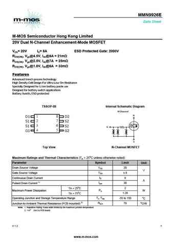
MMN9926E Data Sheet M-MOS Semiconductor Hong Kong Limited 20V Dual N-Channel Enhancement-Mode MOSFET VDS= 20V ID= 8A ESD Protected Gate 2000V RDS(ON), Vgs@4.5V, Ids@8A = 21m RDS(ON), Vgs@2.5V, Ids@7A = 25m RDS(ON), Vgs@1.8V, Ids@6A = 33m Features Advanced trench process technology High Density Cell Design For Ultra Low On-Resistance Specially Designed for Li ion battery pac... See More ⇒
mmn9926.pdf
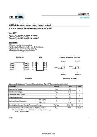
MMN9926 Data Sheet M-MOS Semiconductor Hong Kong Limited 20V N-Channel Enhancement-Mode MOSFET VDS= 20V RDS(ON), Vgs@4.5V, Ids@6A = 30m RDS(ON), Vgs@2.5V, Ids@5.2A = 40m Features Advanced trench process technology High Density Cell Design For Ultra Low On-Resistance High Power and Current handing capability Ideal for Li ion battery pack applications TSSOP-08 SO-8 Internal Sche... See More ⇒
mmn9926bdy.pdf
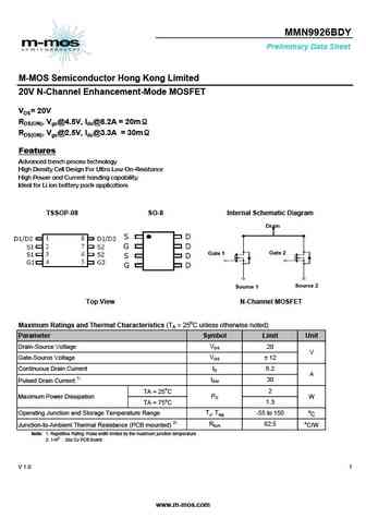
MMN9926BDY Preliminary Data Sheet M-MOS Semiconductor Hong Kong Limited 20V N-Channel Enhancement-Mode MOSFET VDS= 20V RDS(ON), Vgs@4.5V, Ids@8.2A = 20m RDS(ON), Vgs@2.5V, Ids@3.3A = 30m Features Advanced trench process technology High Density Cell Design For Ultra Low On-Resistance High Power and Current handing capability Ideal for Li ion battery pack applications TSSOP-08 S... See More ⇒
nce9926.pdf
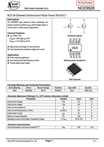
Pb Free Product http //www.ncepower.com NCE9926 NCE N-Channel Enhancement Mode Power MOSFET Description The NCE9926 uses advanced trench technology and design to provide excellent RDS(ON) with low gate charge. It can be used in a wide variety of applications. General Features VDS =20V,ID =6A Schematic diagram RDS(ON) ... See More ⇒
smc9926.pdf
SMC9926 20V Dual N-Channel Enhancement Mode MOSFET DESCRIPTION FEATURE The SMC9926 is the Dual N-Channel logic 20V/8.0A, RDS(ON) =17m (typ.)@VGS =10V enhancement mode power field effect transistor is 20V/7.0A, RDS(ON) =18m (typ.)@VGS =4.5V produced using high cell density. advanced trench 20V/6.0A, RDS(ON) =23m (typ.)@VGS =2.5V technology to provide exce... See More ⇒
ssm9926gm.pdf
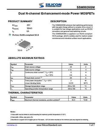
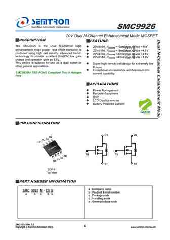
SSM9926GM Dual N-channel Enhancement-mode Power MOSFETs PRODUCT SUMMARY DESCRIPTION The SSM9926GM acheives fast switching performance BVDSS 20V with low gate charge without a complex drive circuit. It RDS(ON) 30m is suitable for low voltage applications such as DC/DC converters and general load-switching circuits. I 6A D The SSM9926GM is supplied in an RoHS-compliant Pb-free; Ro... See More ⇒
ssm9926o.pdf
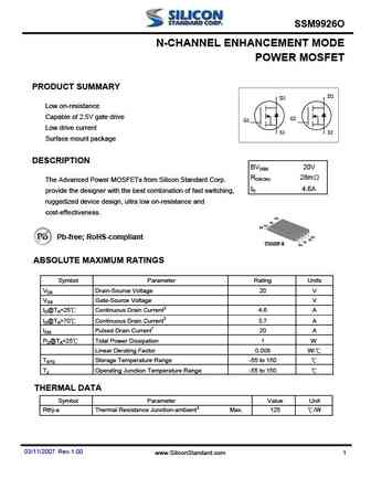
SSM9926O N-CHANNEL ENHANCEMENT MODE POWER MOSFET PRODUCT SUMMARY D2 D1 Low on-resistance Capable of 2.5V gate drive G2 G1 Low drive current S1 S2 Surface mount package DESCRIPTION BVDSS 20V RDS(ON) 28m The Advanced Power MOSFETs from Silicon Standard Corp. ID 4.6A provide the designer with the best combination of fast switching, ruggedized device design, ultra l... See More ⇒
ssm9926tgo.pdf
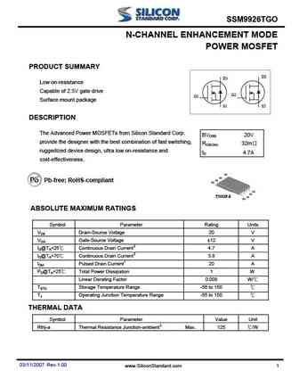
SSM9926TGO N-CHANNEL ENHANCEMENT MODE POWER MOSFET PRODUCT SUMMARY D2 D1 Low on-resistance Capable of 2.5V gate drive G2 G1 Surface mount package S1 S2 DESCRIPTION The Advanced Power MOSFETs from Silicon Standard Corp. BVDSS 20V provide the designer with the best combination of fast switching, RDS(ON) 32m ruggedized device design, ultra low on-resistance and ID 4.... See More ⇒
ssm9926em.pdf
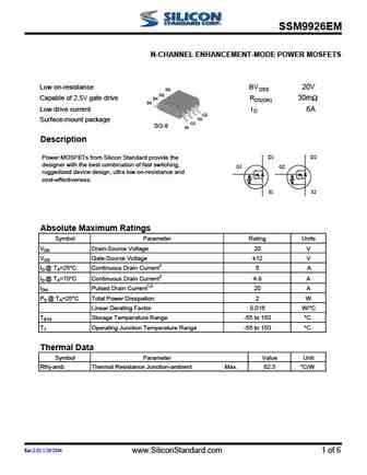
SSM9926EM N-CHANNEL ENHANCEMENT-MODE POWER MOSFETS Low on-resistance BV 20V DSS D2 D2 Capable of 2.5V gate drive D1 RDS(ON) 30m D1 Low drive current I 6A D G2 S2 Surface-mount package G1 SO-8 S1 Description Power MOSFETs from Silicon Standard provide the D1 D2 designer with the best combination of fast switching, G1 G2 ruggedized device design, ultra low on-resistance a... See More ⇒
ssm9926geo.pdf
SSM9926GEO N-CHANNEL ENHANCEMENT-MODE POWER MOSFETS G2 Low on-resistance BV 20V DSS S2 S2 D2 Capable of 2.5V gate drive RDS(ON) 28m G1 S1 Low drive current S1 I 4.6A D TSSOP-8 D1 Surface-mount package Description D1 D2 Power MOSFETs from Silicon Standard provide the G1 G2 designer with the best combination of fast switching, ruggedized device design, ultra low on-resista... See More ⇒
sl9926a.pdf
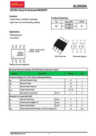
SL9926A 20V/6A Dual N-Channel MOSFET Features Product Summary Trench Power LV MOSFET technology VDS RDS(ON) MAX ID MAX High Power and current handing capability 30m @4.5V D2 20V S1 6A D1 45m @2.5V Application PWM application D1 Load Switch D1 D2 D2 D1 D1 D2 D2 S1 9926A Device code G1 XXXXX Code S2 9926A G2 XXXXX SOP-8 top view Schematic diagram... See More ⇒
es9926.pdf
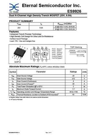
Eternal Semiconductor Inc. ES9926 Dual N-Channel High Density Trench MOSFET (20V, 6.0A) PRODUCT SUMMARY VDSS ID RDS(on) (m )Max 22 @ VGS = 4.5V, ID=6.0A 20V 6.0A 26 @ VGS = 2.5V, ID=5.2A Features Advanced Trench Process Technology High Density Cell Design for Ultra Low On-Resistance Surface mount Package Lead Pb -free and halogen-free Absolute Maximum Ratings ... See More ⇒
9926a.pdf
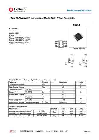
Plastic-Encapsulate Mosfets Dual N-Channel Enhancement Mode Field Effect Transistor 9926A Features VDS (V) = 20V ID = 7A RDS(ON) ... See More ⇒
hsm9926.pdf
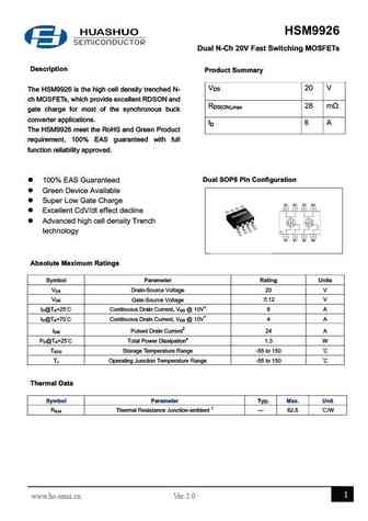
HSM9926 Dual N-Ch 20V Fast Switching MOSFETs Description Product Summary VDS 20 V The HSM9926 is the high cell density trenched N- ch MOSFETs, which provide excellent RDSON and RDS(ON),max 28 m gate charge for most of the synchronous buck converter applications. ID 6 A The HSM9926 meet the RoHS and Green Product requirement, 100% EAS guaranteed with full function rel... See More ⇒
jmtp9926a.pdf
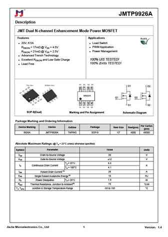
JMTP9926A Description JMT Dual N-channel Enhancement Mode Power MOSFET Features Applications 20V, 6.5A Load Switch RDS(ON) ... See More ⇒
jmtp9926b.pdf

JMTP9926B Description JMT Dual N-channel Enhancement Mode Power MOSFET Features Applications 20V, 6A Load Switch RDS(ON) ... See More ⇒
lpm9926.pdf
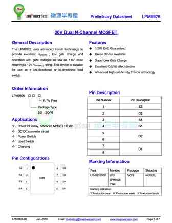
Preliminary Datasheet LPM9926 20V Dual N-Channel MOSFET General Description Features 100% EAS Guaranteed The LPM9926 uses advanced trench technology to provide excellent R , low gate charge and Green Device Available DS(ON) operation with gate voltages as low as 1.8V while Super Low Gate Charge retaining a 12V V rating. This device is suitable GS(MAX) Excelle... See More ⇒
9926a.pdf
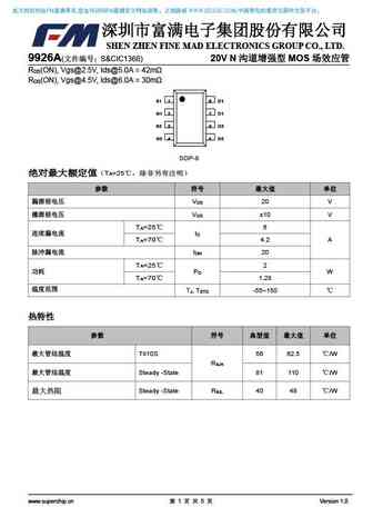
1 2 3 D FM , FM WWW.SZLCSC.COM, SHEN ZHEN FINE MAD ELECTRONICS GROUP CO., LTD. 9926A( S&CIC1368) 20V N MOS R (ON), Vgs@2.5V, Ids@5.0A = 42m DS R (ON), Vgs@4.5V, Ids@6.0A =... See More ⇒
pt9926.pdf
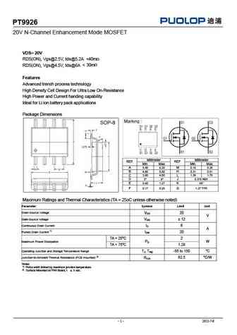
PT9926 20V N-Channel Enhancement Mode MOSFET VDS= 20V RDS(ON), Vgs@2.5V, Ids@5.2A ... See More ⇒
9926b.pdf
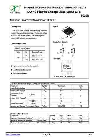
SHENZHEN TUOFENG SEMICONDUCTOR TECHNOLOGY CO.,LTD SOP-8 Plastic-Encapsulate MOSFETS 9926B N-Channel Enhancement Mode Power MOSFET SOP-8L D2 Description D2 D1 The 9926B uses advanced trench technology to provide D1 excellent RDS(ON) and low gate charge . The complementary G2 G S2 MOSFETs may be used to form a level shifted high side G1 S S S1 SO-8 S switch, and for a hos... See More ⇒
9926a.pdf
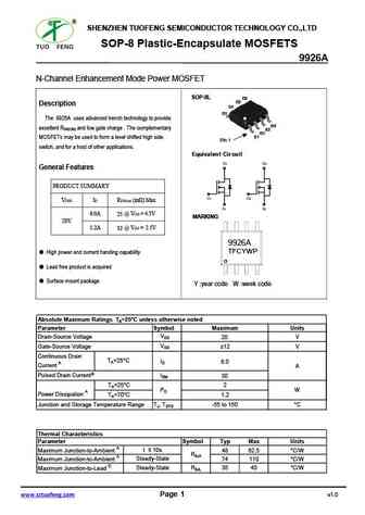
SHENZHEN TUOFENG SEMICONDUCTOR TECHNOLOGY CO.,LTD SOP-8 Plastic-Encapsulate MOSFETS 9926A N-Channel Enhancement Mode Power MOSFET SOP-8L D2 D2 Description D1 D1 The 9926A uses advanced trench technology to provide G2 excellent RDS(ON) and low gate charge . The complementary G S2 G1 S S S1 MOSFETs may be used to form a level shifted high side SO-8 S Pin 1 switch, and fo... See More ⇒
wsp9926a.pdf

WSP9926A Dual N-Channel MOSFET General Description Product Summery The WSP9926A is the highest performance BVDSS RDSON ID trench N-ch MOSFET with extreme high cell density , which provide excellent RDSON 20V 20m 7.5A and gate charge for most of the small power switching and load switch applications. Applications The WSP9926A meet the RoHS and Green Product requirement w... See More ⇒
wsp9926b.pdf
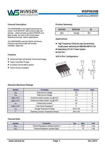
WSP9926B Dual N-Channel MOSFET General Description Product Summery The WSP9926B is the highest performance BVDSS RDSON ID trench N-ch MOSFET with extreme high cell density , which provide excellent RDSON and 20V 17m 8A gate charge for most of the small power switching and load switch applications. Applications The WSP9926B meet the RoHS and Green Product requirement wit... See More ⇒
se9926.pdf
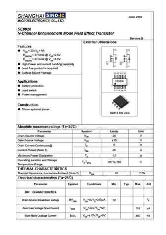
SHANGHAI June 2006 MICROELECTRONICS CO., LTD. SE9926 N-Channel Enhancement Mode Field Effect Transistor Revision B External Dimensions Features VDS = 20V,ID = 6A RDS(ON) ... See More ⇒
sm9926.pdf
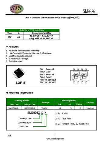
SM9926 Dual N-Channel Enhancement-Mode MOSFET(20V, 6A) PRODUCT SUMMARY VDSS ID RDS(on) (m-ohm) Max 28 @ VGS = 4.5V, ID=6A 20V 6A 40 @ VGS =2.5V,ID=5.2A Features 1 Advanced Trench Process Technology. 2 High Density Cell Design for Ultra Low On-Resistance. 3 Lead free product is acquired. 4 Surface mount Package. 5 RoHS Compliant. Pin 1 Source1 Pin 2 Ga... See More ⇒
cem9926.pdf
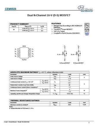
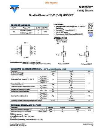
CEM9926 www.VBsemi.tw Dual N-Channel 20-V (D-S) MOSFET FEATURES PRODUCT SUMMARY Halogen-free According to IEC 61249-2-21 VDS (V) RDS(on) ( )ID (A) Definition 0.025 at VGS = 4.5 V 7.1 TrenchFET Power MOSFET 20 0.035 at VGS = 2.5 V 6.0 100 % Rg Tested Compliant to RoHS Directive 2002/95/EC SO-8 D1 D2 S1 1 D1 8 G1 2 D1 7 S2 3 D2 6 G1 G2 G2 4 D2 ... See More ⇒
fds9926a.pdf

FDS9926A www.VBsemi.tw Dual N-Channel 20-V (D-S) MOSFET FEATURES PRODUCT SUMMARY Halogen-free According to IEC 61249-2-21 VDS (V) RDS(on) ( )ID (A) Definition 0.025 at VGS = 4.5 V 7.1 TrenchFET Power MOSFET 20 0.035 at VGS = 2.5 V 6.0 100 % Rg Tested Compliant to RoHS Directive 2002/95/EC SO-8 D1 D2 S1 1 D1 8 G1 2 D1 7 S2 3 D2 6 G1 G2 G2 4 D2... See More ⇒
sdm9926.pdf

SDM9926 www.VBsemi.tw Dual N-Channel 20-V (D-S) MOSFET FEATURES PRODUCT SUMMARY Halogen-free According to IEC 61249-2-21 VDS (V) RDS(on) ( )ID (A) Definition 0.025 at VGS = 4.5 V 7.1 TrenchFET Power MOSFET 20 0.035 at VGS = 2.5 V 6.0 100 % Rg Tested Compliant to RoHS Directive 2002/95/EC SO-8 D1 D2 S1 1 D1 8 G1 2 D1 7 S2 3 D2 6 G1 G2 G2 4 D2 ... See More ⇒
me9926.pdf
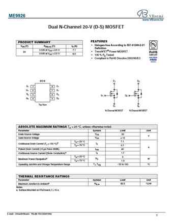
ME9926 www.VBsemi.tw Dual N-Channel 20-V (D-S) MOSFET FEATURES PRODUCT SUMMARY Halogen-free According to IEC 61249-2-21 VDS (V) RDS(on) ( )ID (A) Definition 0.025 at VGS = 4.5 V 7.1 TrenchFET Power MOSFET 20 0.035 at VGS = 2.5 V 6.0 100 % Rg Tested Compliant to RoHS Directive 2002/95/EC SO-8 D1 D2 S1 1 D1 8 G1 2 D1 7 S2 3 D2 6 G1 G2 G2 4 D2 ... See More ⇒
vbza9926.pdf
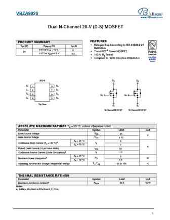
VBZA9926 www.VBsemi.com Dual N-Channel 20-V (D-S) MOSFET FEATURES PRODUCT SUMMARY Halogen-free According to IEC 61249-2-21 VDS (V) RDS(on) ( )ID (A) Definition 0.015at VGS = 10 V 8 TrenchFET Power MOSFET 20 0.023 at VGS = 4.5 V 5.5 100 % Rg Tested Compliant to RoHS Directive 2002/95/EC SO-8 D1 D2 S1 1 D1 8 G1 2 D1 7 S2 3 D2 6 G1 G2 G2 4 D2 5 Top... See More ⇒
vbza9926a.pdf
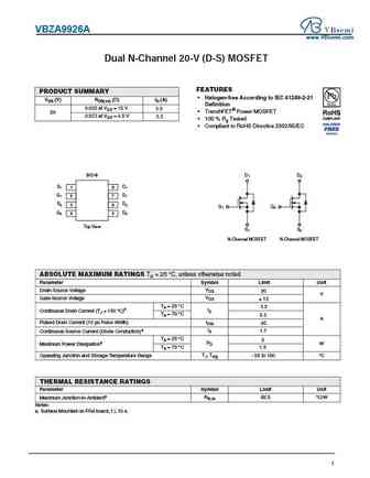
VBZA9926A www.VBsemi.com Dual N-Channel 20-V (D-S) MOSFET FEATURES PRODUCT SUMMARY Halogen-free According to IEC 61249-2-21 VDS (V) RDS(on) ( )ID (A) Definition 0.020 at VGS = 10 V 5.8 TrenchFET Power MOSFET 20 0.023 at VGS = 4.5 V 5.5 100 % Rg Tested Compliant to RoHS Directive 2002/95/EC SO-8 D1 D2 S1 1 D1 8 G1 2 D1 7 S2 3 D2 6 G1 G2 G2 4 D2 5 ... See More ⇒
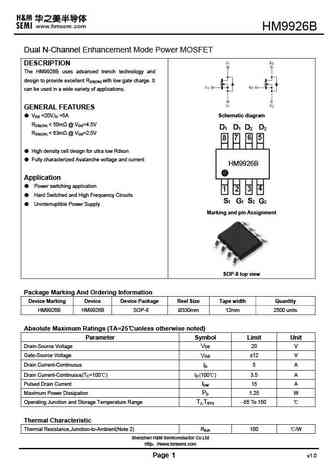
hm9926.pdf

HM9926 Dual N-Channel Enhancement Mode Power MOSFET DESCRIPTION The HM9926 uses advanced trench technology and design to provide excellent RDS(ON) with low gate charge. It can be used in a wide variety of applications. GENERAL FEATURES VDS =20V,ID =6A Schematic diagram RDS(ON) ... See More ⇒
hm9926b.pdf
HM9926B Dual N-Channel Enhancement Mode Power MOSFET DESCRIPTION The HM9926B uses advanced trench technology and design to provide excellent RDS(ON) with low gate charge. It can be used in a wide variety of applications. GENERAL FEATURES VDS =20V,ID =5A Schematic diagram RDS(ON) ... See More ⇒
ap9926a.pdf
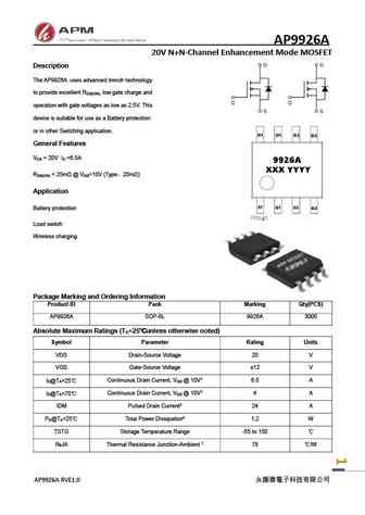
AP9926A 20V N+N-Channel Enhancement Mode MOSFET Description The AP9926A uses advanced trench technology to provide excellent R , low gate charge and DS(ON) operation with gate voltages as low as 2.5V. This device is suitable for use as a Battery protection or in other Switching application. General Features V = 20V I =6.5A DS D R ... See More ⇒
Detailed specifications: 2N6847U, 2303, 2304, 2305, 4414, 4614, 4800, 8958, 4N60, 045Y, 06N03, 10N60A, 10N60AF, 10N60H, 10N80AF, 10N80B, 10N90A
Keywords - 9926 MOSFET specs
9926 cross reference
9926 equivalent finder
9926 pdf lookup
9926 substitution
9926 replacement
Step-by-step guide to finding a MOSFET replacement. Cross-reference parts and ensure compatibility for your repair or project.
History: HYG035N10NS2B | SLD40N03TB | SLD10N65U | SM1F12NSUB | STD155N3H6 | SLD140N03TB | SLF65R380E7C
🌐 : EN ES РУ

LIST
Last Update
MOSFET: AUB034N10 | AUB033N08BG | AUB026N085 | AUA062N08BG | AUA060N08AG | AUA056N08BGL | AUA039N10 | ASW80R290E | ASW65R120EFD | ASW65R110E
Popular searches
irfz44n mosfet | lm317t datasheet | irf540 | bc337 | ksc1845 | c1815 transistor | 2sc1815 | irfz44