10N90A Specs and Replacement
Type Designator: 10N90A
Type of Transistor: MOSFET
Type of Control Channel: N-Channel
Absolute Maximum Ratings
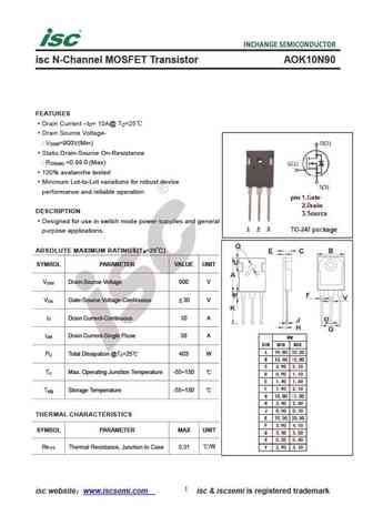
Pd ⓘ - Maximum Power Dissipation: 300 W
|Vds|ⓘ - Maximum Drain-Source Voltage: 900 V
|Vgs|ⓘ - Maximum Gate-Source Voltage: 20 V
|Id| ⓘ - Maximum Drain Current: 10 A
Tj ⓘ - Maximum Junction Temperature: 150 °C
Electrical Characteristics
tr ⓘ - Rise Time: 15 nS
Cossⓘ - Output Capacitance: 315 pF
RDSonⓘ - Maximum Drain-Source On-State Resistance: 1.1 Ohm
Package: LCC
10N90A substitution
- MOSFET ⓘ Cross-Reference Search
10N90A datasheet
10n90a msafx10n90a.pdf
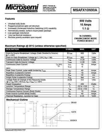
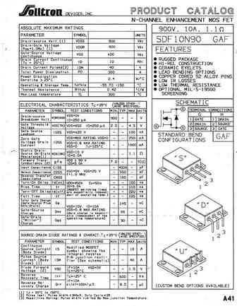
2830 S. Fairview St. Santa Ana, CA 92704 PH (714) 979-8220 FAX (714) 966-5256 MSAFX10N90A Features 900 Volts Ultrafast body diode 10 Amps Rugged polysilicon gate cell structure Increased Unclamped Inductive Switching (UIS) capability 1.1 Hermetically sealed, surface mount power package Low package inductance Very low thermal resistance N-CHANNEL Rev... See More ⇒
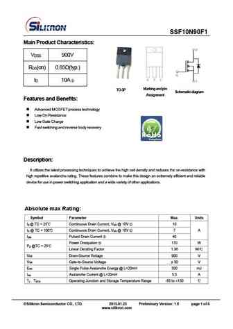
ssf10n90a.pdf
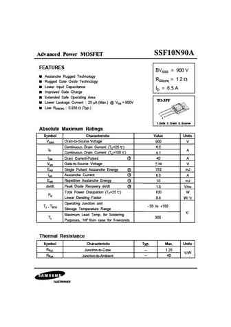
Advanced Power MOSFET FEATURES BVDSS = 900 V Avalanche Rugged Technology RDS(on) = 1.2 Rugged Gate Oxide Technology Lower Input Capacitance ID = 6.5 A Improved Gate Charge Extended Safe Operating Area Lower Leakage Current 25 A (Max.) @ VDS = 900V Low RDS(ON) 0.938 (Typ.) 1 2 3 1.Gate 2. Drain 3. Source Absolute Maximum Ratings Symbol Characteristic Valu... See More ⇒
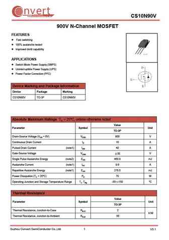
ssh10n90a.pdf
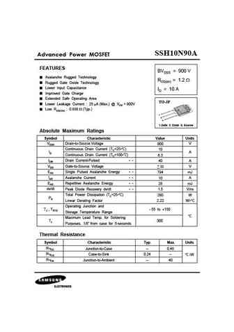
SSH10N90A Advanced Power MOSFET FEATURES BVDSS = 900 V Avalanche Rugged Technology RDS(on) = 1.2 Rugged Gate Oxide Technology Lower Input Capacitance ID = 10 A Improved Gate Charge Extended Safe Operating Area TO-3P Lower Leakage Current 25 A (Max.) @ VDS = 900V Low RDS(ON) 0.938 (Typ.) 1 2 3 1.Gate 2. Drain 3. Source Absolute Maximum Ratings Symbol Char... See More ⇒
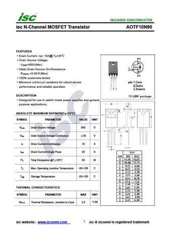
ixfh10n90 ixfm10n90 ixfh12n90 ixfm12n90 ixfh13n90 ixfm13n90.pdf
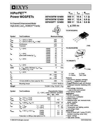
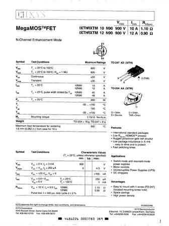
VDSS ID25 RDS(on) HiPerFETTM IXFH/IXFM 10 N90 900 V 10 A 1.1 Power MOSFETs IXFH/IXFM 12 N90 900 V 12 A 0.9 IXFH/IXFT 13 N90 900 V 13 A 0.8 N-Channel Enhancement Mode 250 ns High dv/dt, Low trr, HDMOSTM Family trr TO-247 AD (IXFH) Symbol Test Conditions Maximum Ratings VDSS TJ = 25 C to 1... See More ⇒
Detailed specifications: 9926, 045Y, 06N03, 10N60A, 10N60AF, 10N60H, 10N80AF, 10N80B, AO3407, 11N10, 11N10G, 11P50A, 12N50A, 12N60A, 12N60AF, 13N110A, 13N60A
Keywords - 10N90A MOSFET specs
10N90A cross reference
10N90A equivalent finder
10N90A pdf lookup
10N90A substitution
10N90A replacement
Step-by-step guide to finding a MOSFET replacement. Cross-reference parts and ensure compatibility for your repair or project.
History: AOD294A | APQ04SN60CH
🌐 : EN ES РУ

LIST
Last Update
MOSFET: AUB034N10 | AUB033N08BG | AUB026N085 | AUA062N08BG | AUA060N08AG | AUA056N08BGL | AUA039N10 | ASW80R290E | ASW65R120EFD | ASW65R110E
Popular searches
2n5551 | irf540n | irf3205 mosfet | 2n3055 | irfp260n | 2n2222 datasheet | irf9540 | 2n3055 datasheet