60N05 Specs and Replacement
Type Designator: 60N05
Type of Transistor: MOSFET
Type of Control Channel: N-Channel
Absolute Maximum Ratings
Pd ⓘ
- Maximum Power Dissipation: 150 W
|Vds|ⓘ - Maximum Drain-Source Voltage: 50 V
|Vgs|ⓘ - Maximum Gate-Source Voltage: 20 V
|Id| ⓘ - Maximum Drain Current: 60 A
Tj ⓘ - Maximum Junction Temperature: 150 °C
Electrical Characteristics
tr ⓘ - Rise Time: 17 nS
Cossⓘ -
Output Capacitance: 169 pF
RDSonⓘ - Maximum Drain-Source On-State Resistance: 0.014 Ohm
Package: TO-220C
- MOSFET ⓘ Cross-Reference Search
60N05 datasheet
..1. Size:236K inchange semiconductor
60n05.pdf 
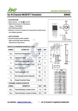
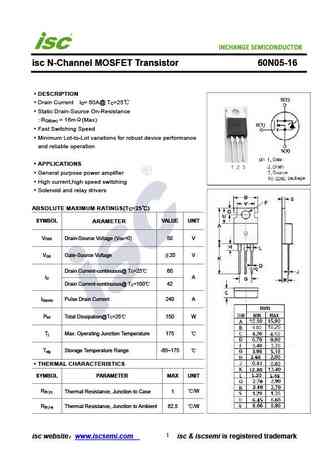
INCHANGE Semiconductor isc N-Channel MOSFET Transistor 60N05 DESCRIPTION Drain Current I = 60A@ T =25 D C Static Drain-Source On-Resistance R = 18m (Max) DS(on) Fast Switching Speed Minimum Lot-to-Lot variations for robust device performance and reliable operation APPLICATIONS General purpose power amplifier High current,high speed switching Solenoid and relay ... See More ⇒
0.2. Size:216K motorola
mtb60n05hdl.pdf
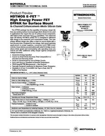
MOTOROLA Order this document SEMICONDUCTOR TECHNICAL DATA by MTB60N05HDL/D Product Preview MTB60N05HDL HDTMOS E-FET. Motorola Preferred Device High Energy Power FET D2PAK for Surface Mount TMOS POWER FET 60 AMPERES N Channel Enhancement Mode Silicon Gate 50 VOLTS The D2PAK package has the capability of housing a larger die RDS(on) = 0.014 OHM than any existing surface mou... See More ⇒
0.3. Size:171K motorola
mtp60n05hdl.pdf

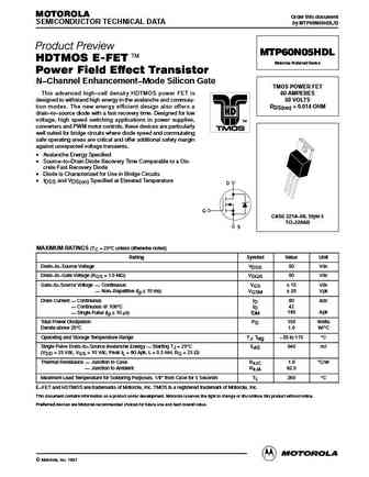
MOTOROLA Order this document SEMICONDUCTOR TECHNICAL DATA by MTP60N05HDL/D Product Preview MTP60N05HDL HDTMOS E-FET. Motorola Preferred Device Power Field Effect Transistor N Channel Enhancement Mode Silicon Gate TMOS POWER FET This advanced high cell density HDTMOS power FET is 60 AMPERES designed to withstand high energy in the avalanche and commuta- 50 VOLTS tion modes.... See More ⇒
0.4. Size:166K motorola
mtp60n05hdlrev0.pdf
MOTOROLA Order this document SEMICONDUCTOR TECHNICAL DATA by MTP60N05HDL/D Product Preview MTP60N05HDL HDTMOS E-FET. Motorola Preferred Device Power Field Effect Transistor N Channel Enhancement Mode Silicon Gate TMOS POWER FET This advanced high cell density HDTMOS power FET is 60 AMPERES designed to withstand high energy in the avalanche and commuta- 50 VOLTS tion modes.... See More ⇒
0.5. Size:77K st
stp60n05 stp60n06.pdf

STP60N05-14 STP60N06-14 N - CHANNEL ENHANCEMENT MODE POWER MOS TRANSISTOR PRELIMINARY DATA TYPE V R I DSS DS(on) D STP60N05-14 50 V ... See More ⇒
0.6. Size:81K st
stp60n05-14.pdf

STP60N05-14 STP60N06-14 N - CHANNEL ENHANCEMENT MODE POWER MOS TRANSISTOR PRELIMINARY DATA TYPE V R I DSS DS(on) D STP60N05-14 50 V ... See More ⇒
0.8. Size:54K st
stp60n05-14 stp60n06-14.pdf
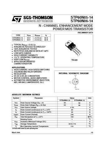
STP60N05-14 STP60N06-14 N - CHANNEL ENHANCEMENT MODE POWER MOS TRANSISTOR PRELIMINARY DATA TYPE V R I DSS DS(on) D STP60N05-14 50 V ... See More ⇒
0.9. Size:354K st
stp60n05-16 stp60n06-16.pdf
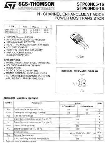
www.DataSheet4U.com www.DataSheet4U.com www.DataSheet4U.com www.DataSheet4U.com www.DataSheet4U.com www.DataSheet4U.com www.DataSheet4U.com ... See More ⇒
0.11. Size:102K renesas
np60n055vuk.pdf
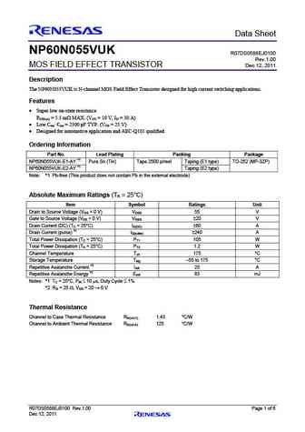
Preliminary Data Sheet NP60N055VUK R07DS0588EJ0100 Rev.1.00 MOS FIELD EFFECT TRANSISTOR Dec 12, 2011 Description The NP60N055VUK is N-channel MOS Field Effect Transistor designed for high current switching applications. Features Super low on-state resistance RDS(on) = 5.5 m MAX. (VGS = 10 V, ID = 30 A) Low Ciss Ciss = 2500 pF TYP. (VDS = 25 V) Designed for au... See More ⇒
0.12. Size:260K renesas
np60n055kug.pdf
To our customers, Old Company Name in Catalogs and Other Documents On April 1st, 2010, NEC Electronics Corporation merged with Renesas Technology Corporation, and Renesas Electronics Corporation took over all the business of both companies. Therefore, although the old company name remains in this document, it is a valid Renesas Electronics document. We appreciate your understanding. ... See More ⇒
0.13. Size:102K renesas
np160n055tuk.pdf
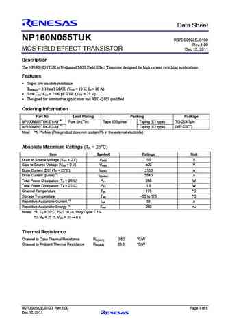
Preliminary Data Sheet NP160N055TUK R07DS0592EJ0100 Rev.1.00 MOS FIELD EFFECT TRANSISTOR Dec 12, 2011 Description The NP160N055TUK is N-channel MOS Field Effect Transistor designed for high current switching applications. Features Super low on-state resistance RDS(on) = 2.10 m MAX. (VGS = 10 V, ID = 80 A) Low Ciss Ciss = 7500 pF TYP. (VDS = 25 V) Designed for... See More ⇒
0.14. Size:207K renesas
np160n055tuj.pdf
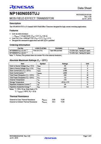
Preliminary Data Sheet NP160N055TUJ R07DS0022EJ0100 Rev.1.00 MOS FIELD EFFECT TRANSISTOR Jul 01, 2010 Description The NP160N055TUJ is N-channel MOS Field Effect Transistor designed for high current switching applications. Features Low on-state resistance RDS(on) = 3.0 m MAX. (VGS = 10 V, ID = 80 A) Low Ciss Ciss = 6900 pF TYP. (VDS = 25 V, VGS = 0 V) Desig... See More ⇒
0.15. Size:103K renesas
np60n055muk np60n055nuk.pdf
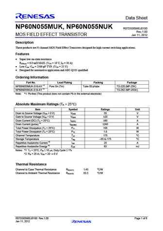
Preliminary Data Sheet NP60N055MUK, NP60N055NUK R07DS0598EJ0100 Rev.1.00 MOS FIELD EFFECT TRANSISTOR Jan 11, 2012 Description These products are N-channel MOS Field Effect Transistors designed for high current switching applications. Features Super low on-state resistance RDS(on) = 6.0 m MAX. (VGS = 10 V, ID = 30 A) Low Ciss Ciss = 2500 pF TYP. (VDS = 25 V) D... See More ⇒
0.18. Size:248K ixys
ixta260n055t2 ixtp260n055t2.pdf
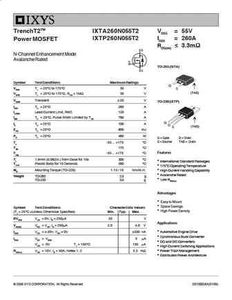
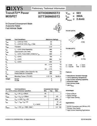
TrenchT2TM IXTA260N055T2 VDSS = 55V IXTP260N055T2 ID25 = 260A Power MOSFET RDS(on) 3.3m N-Channel Enhancement Mode Avalanche Rated TO-263 (IXTA) Symbol Test Conditions Maximum Ratings G VDSS TJ = 25 C to 175 C 55 V S (TAB) VDGR TJ = 25 C to 175 C, RGS = 1M 55 V VGSM Transient 20 V TO-220 (IXTP) ID25 TC = 25 C 260 A ILRM... See More ⇒
0.19. Size:166K ixys
ixth260n055t2.pdf
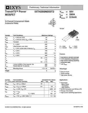
Preliminary Technical Information VDSS = 55V TrenchT2TM Power IXTH260N055T2 ID25 = 260A MOSFET RDS(on) 3.3m N-Channel Enhancement Mode Avalanche Rated TO-247 Symbol Test Conditions Maximum Ratings VDSS TJ = 25 C to 175 C55 V G VDGR TJ = 25 C to 175 C, RGS = 1M 55 V (TAB) D S VGSM Transient 20 V ID25 TC = 25 C 260 A G = Gate D =... See More ⇒
0.20. Size:1094K cn anhi
aud060n055 aun042n055 aub050n055 aup060n055.pdf
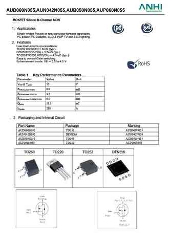
AUD060N055,AUN042N055,AUB050N055,AUP060N055 MOSFET Silicon N-Channel MOS 1. Applications Single-ended flyback or two-transistor forward topologies. PC power, PD Adaptor, LCD & PDP TV and LED lighting. 2. Features Low drain-source on-resistance TO252 RDS(ON) = 4m (typ.) DFN5X6 RDS(ON) = 3.6m (typ.) TO263&TO220 RDS(ON) = 4.3m (typ.) Easy to control Gate switching Enhancement... See More ⇒
0.21. Size:1263K cn hmsemi
hm60n05k.pdf
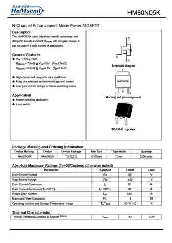
HM60N05K N-Channel Enhancement Mode Power MOSFET Description The HM60N05K uses advanced trench technology and design to provide excellent RDS(ON) with low gate charge. It can be used in a wide variety of applications. General Features VDS = 50V,ID =60A RDS(ON) ... See More ⇒
0.22. Size:1063K cn hmsemi
hm60n05.pdf
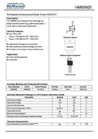
HM60N05 N-Channel Enhancement Mode Power MOSFET Description The HM60N05 uses advanced trench technology and design to provide excellent RDS(ON) with low gate charge. It can be used in a wide variety of applications. General Features VDS = 50V,ID =60A RDS(ON) ... See More ⇒
0.23. Size:230K inchange semiconductor
60n05-16.pdf
INCHANGE Semiconductor isc N-Channel MOSFET Transistor 60N05-16 DESCRIPTION Drain Current I = 60A@ T =25 D C Static Drain-Source On-Resistance R = 16m (Max) DS(on) Fast Switching Speed Minimum Lot-to-Lot variations for robust device performance and reliable operation APPLICATIONS General purpose power amplifier High current,high speed switching Solenoid and... See More ⇒
Detailed specifications: 2SK1938-01, 2SK1939-01, 2SK1982-01M, 2SK2020-01MR, 2SK2645, 2SK2850, 40N10, 50N15, IRLB4132, 60N05-16, 60N06-18, 60N10, 6N70A, 75N06, 75N10, 75NF75, BUK436-100A
Keywords - 60N05 MOSFET specs
60N05 cross reference
60N05 equivalent finder
60N05 pdf lookup
60N05 substitution
60N05 replacement
Step-by-step guide to finding a MOSFET replacement. Cross-reference parts and ensure compatibility for your repair or project.