TK17A65W Specs and Replacement
Type Designator: TK17A65W
Type of Transistor: MOSFET
Type of Control Channel: N-Channel
Absolute Maximum Ratings
Pd ⓘ - Maximum Power Dissipation: 45 W
|Vds|ⓘ - Maximum Drain-Source Voltage: 650 V
|Vgs|ⓘ - Maximum Gate-Source Voltage: 30 V
|Id| ⓘ - Maximum Drain Current: 17.3 A
Tj ⓘ - Maximum Junction Temperature: 150 °C
Electrical Characteristics
tr ⓘ - Rise Time: 15 nS
Cossⓘ - Output Capacitance: 40 pF
RDSonⓘ - Maximum Drain-Source On-State Resistance: 0.2 Ohm
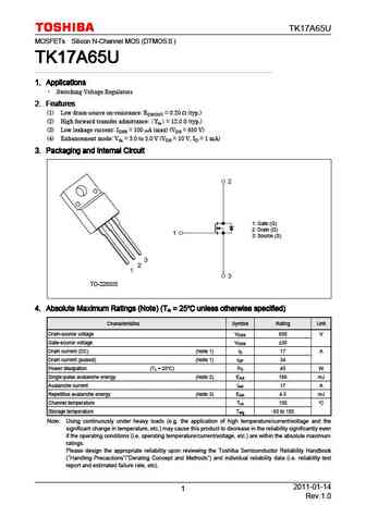
Package: TO-220F
TK17A65W substitution
- MOSFET ⓘ Cross-Reference Search
TK17A65W datasheet
tk17a65w.pdf
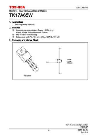
TK17A65W MOSFETs Silicon N-Channel MOS (DTMOS ) TK17A65W TK17A65W TK17A65W TK17A65W 1. Applications 1. Applications 1. Applications 1. Applications Switching Voltage Regulators 2. Features 2. Features 2. Features 2. Features (1) Low drain-source on-resistance RDS(ON) = 0.17 (typ.) by used to Super Junction Structure DTMOS (2) Easy to control Gate switching (3) En... See More ⇒
tk17a65w.pdf
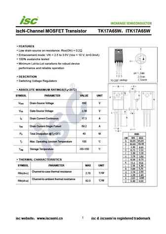
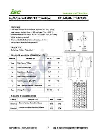
INCHANGE Semiconductor iscN-Channel MOSFET Transistor TK17A65W ITK17A65W FEATURES Low drain-source on-resistance RDS(ON) = 0.2 Enhancement mode Vth = 2.5 to 3.5V (VDS = 10 V, ID=0.9mA) 100% avalanche tested Minimum Lot-to-Lot variations for robust device performance and reliable operation DESCRITION Switching Voltage Regulators ABSOLUTE MAXIMUM RATINGS(T =25 )... See More ⇒
tk17a65w5.pdf
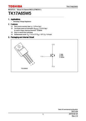
TK17A65W5 MOSFETs Silicon N-Channel MOS (DTMOS ) TK17A65W5 TK17A65W5 TK17A65W5 TK17A65W5 1. Applications 1. Applications 1. Applications 1. Applications Switching Voltage Regulators 2. Features 2. Features 2. Features 2. Features (1) Fast reverse recovery time trr = 110 ns (typ.) (2) Low drain-source on-resistance RDS(ON) = 0.19 (typ.) by used to Super Junction Str... See More ⇒
tk17a65w5.pdf
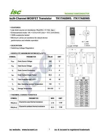
INCHANGE Semiconductor iscN-Channel MOSFET Transistor TK17A65W5 ITK17A65W5 FEATURES Low drain-source on-resistance RDS(ON) = 0.19 (typ.) Enhancement mode Vth = 3.0 to 4.5V (VDS = 10 V, ID=0.9mA) 100% avalanche tested Minimum Lot-to-Lot variations for robust device performance and reliable operation DESCRITION Switching Voltage Regulators ABSOLUTE MAXIMUM RATINGS... See More ⇒
Detailed specifications: IRL8114, TK10A50W, TK10A60D5, TK10A80W, TK10E80W, TK12A50D5, TK12A50W, TK12A80W, IRLZ44N, TK17A65W5, TK17E80W, TK19A50W, TK22A65X5, TK290A60Y, TK290A65Y, TK380A60Y, TK380A65Y
Keywords - TK17A65W MOSFET specs
TK17A65W cross reference
TK17A65W equivalent finder
TK17A65W pdf lookup
TK17A65W substitution
TK17A65W replacement
Learn how to find the right MOSFET substitute. A guide to cross-reference, check specs and replace MOSFETs in your circuits.
History: APM9946J | IRLL014PBF | IRFH8318 | LSC80R350GT | HUF76645SF085 | LSD65R180GT | IRFH5406
🌐 : EN ES РУ

LIST
Last Update
MOSFET: ASU70R600E | ASU65R850E | ASU65R550E | ASU65R350E | ASR65R120EFD | ASR65R046EFD | ASQ65R046EFD | ASM65R280E | ASM60R330E | ASE70R950E
Popular searches
ksc1845 transistor | irf630 datasheet | mpsa13 equivalent | c5198 | 2sc1969 transistor | bcy21 | s8550 datasheet | mj50ac100