TK19A50W Specs and Replacement
Type Designator: TK19A50W
Type of Transistor: MOSFET
Type of Control Channel: N-Channel
Absolute Maximum Ratings
Pd ⓘ - Maximum Power Dissipation: 40 W
|Vds|ⓘ - Maximum Drain-Source Voltage: 500 V
|Vgs|ⓘ - Maximum Gate-Source Voltage: 30 V
|Id| ⓘ - Maximum Drain Current: 18.5 A
Tj ⓘ - Maximum Junction Temperature: 150 °C
Electrical Characteristics
tr ⓘ - Rise Time: 25 nS
Cossⓘ - Output Capacitance: 35 pF
RDSonⓘ - Maximum Drain-Source On-State Resistance: 0.19 Ohm
Package: TO-220F
TK19A50W substitution
- MOSFET ⓘ Cross-Reference Search
TK19A50W datasheet
tk19a50w.pdf
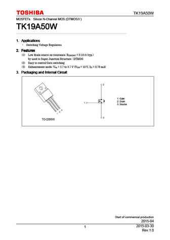
TK19A50W MOSFETs Silicon N-Channel MOS (DTMOS ) TK19A50W TK19A50W TK19A50W TK19A50W 1. Applications 1. Applications 1. Applications 1. Applications Switching Voltage Regulators 2. Features 2. Features 2. Features 2. Features (1) Low drain-source on-resistance RDS(ON) = 0.16 (typ.) by used to Super Junction Structure DTMOS (2) Easy to control Gate switching (3) En... See More ⇒
tk19a50w.pdf
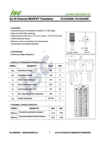
INCHANGE Semiconductor isc N-Channel MOSFET Transistor TK19A50W, ITK19A50W FEATURES Low drain-source on-resistance RDS(ON) = 0.16 (typ.) Easy to control Gate switching Enhancement mode Vth = 2.7 to 3.7 V (VDS = 10 V, ID=0.79 mA) 100% avalanche tested Minimum Lot-to-Lot variations for robust device performance and reliable operation DESCRITION Switching Voltage Reg... See More ⇒
tk19a45d.pdf
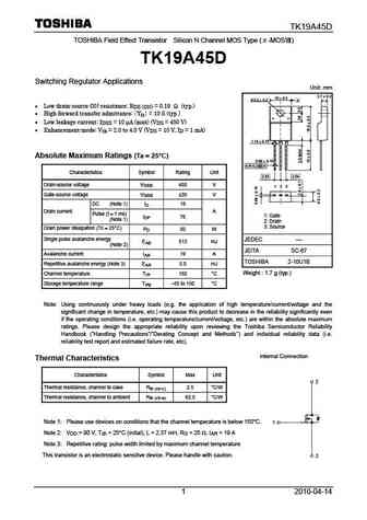
TK19A45D TOSHIBA Field Effect Transistor Silicon N Channel MOS Type ( -MOS ) TK19A45D Switching Regulator Applications Unit mm 2.7 0.2 10 0.3 3.2 0.2 A Low drain-source ON-resistance RDS (ON) = 0.19 (typ.) High forward transfer admittance Yfs = 10 S (typ.) Low leakage current IDSS = 10 A (max) (VDS = 450 V) Enhancement-mode ... See More ⇒
Detailed specifications: TK10A80W, TK10E80W, TK12A50D5, TK12A50W, TK12A80W, TK17A65W, TK17A65W5, TK17E80W, IRFP260N, TK22A65X5, TK290A60Y, TK290A65Y, TK380A60Y, TK380A65Y, TK3A90E, TK3R1A04PL, TK3R3A06PL
Keywords - TK19A50W MOSFET specs
TK19A50W cross reference
TK19A50W equivalent finder
TK19A50W pdf lookup
TK19A50W substitution
TK19A50W replacement
Step-by-step guide to finding a MOSFET replacement. Cross-reference parts and ensure compatibility for your repair or project.
History: LSC80R350GT | TK22A65X5 | IRFH8318 | LSD65R180GT | IRFH5406
🌐 : EN ES РУ

LIST
Last Update
MOSFET: ASU70R600E | ASU65R850E | ASU65R550E | ASU65R350E | ASR65R120EFD | ASR65R046EFD | ASQ65R046EFD | ASM65R280E | ASM60R330E | ASE70R950E
Popular searches
c5198 | 2sc1969 transistor | bcy21 | s8550 datasheet | mj50ac100 | 2sc1318 replacement | 2n3905 | mj15023