IPB07N03L Specs and Replacement
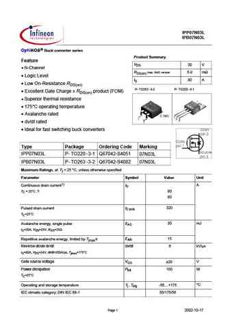
Type Designator: IPB07N03L
Type of Transistor: MOSFET
Type of Control Channel: N-Channel
Absolute Maximum Ratings
Pd ⓘ - Maximum Power Dissipation: 150 W
|Vds|ⓘ - Maximum Drain-Source Voltage: 30 V
|Vgs|ⓘ - Maximum Gate-Source Voltage: 20 V
|Id| ⓘ - Maximum Drain Current: 80 A
Tj ⓘ - Maximum Junction Temperature: 175 °C
Electrical Characteristics
tr ⓘ - Rise Time: 23 nS
Cossⓘ - Output Capacitance: 740 pF
RDSonⓘ - Maximum Drain-Source On-State Resistance: 0.01 Ohm
Package: TO-263
IPB07N03L substitution
- MOSFET ⓘ Cross-Reference Search
IPB07N03L datasheet
ipp07n03l ipb07n03l.pdf
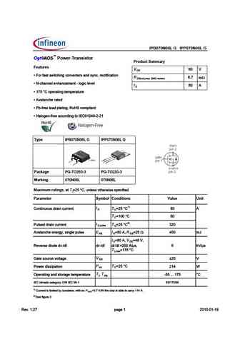
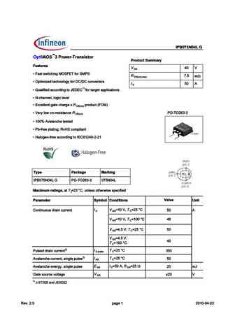
IPP07N03L IPB07N03L OptiMOS Buck converter series Product Summary Feature VDS 30 V N-Channel RDS(on) max. SMD version 5.9 m Logic Level ID 80 A Low On-Resistance RDS(on) P- TO263 -3-2 P- TO220 -3-1 Excellent Gate Charge x RDS(on) product (FOM) Superior thermal resistance 175 C operating temperature Avalanche rated dv/dt rated Ideal for f... See More ⇒
ipb073n15n5.pdf
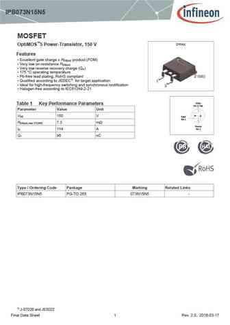
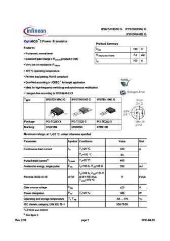
IPB073N15N5 MOSFET D PAK OptiMOS 5 Power-Transistor, 150 V Features Excellent gate charge x R product (FOM) DS(on) Very low on-resistance R DS(on) Very low reverse recovery charge (Q ) rr 175 C operating temperature Pb-free lead plating; RoHS compliant Qualified according to JEDEC1) for target application Ideal for high-frequency switching and synch... See More ⇒
ipb070n06ng ipp070n06ng ipi070n06ngrev1.4.pdf
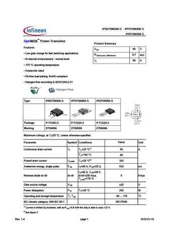
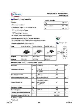
IPB070N06N G IPP070N06N G IPI070N06N G Power-Transistor Product Summary Features V D P &?F 71C5 381A75 6?A 61BC BF9C389>7 1@@B R 7 m , ?> =1G ,' E5AB9?> P ( 381>>581>35=5>C >?A=1... See More ⇒
Detailed specifications: HY3810PS, HY3810PM, HY3906P, HY3906B, HYG067N07NQ1P, HYG067N07NQ1B, HYG067N07NQ1PS, IPP07N03L, IRFB3607, IPW60R060P7, SVF4N65T, SVF4N65F, SVF4N65FG, SVF4N65M, VP0300M, CEPF630, CEBF630
Keywords - IPB07N03L MOSFET specs
IPB07N03L cross reference
IPB07N03L equivalent finder
IPB07N03L pdf lookup
IPB07N03L substitution
IPB07N03L replacement
Learn how to find the right MOSFET substitute. A guide to cross-reference, check specs and replace MOSFETs in your circuits.
🌐 : EN ES РУ
LIST
Last Update
MOSFET: ASU70R600E | ASU65R850E | ASU65R550E | ASU65R350E | ASR65R120EFD | ASR65R046EFD | ASQ65R046EFD | ASM65R280E | ASM60R330E | ASE70R950E
Popular searches
irf640 datasheet | c945 transistor equivalent | irfz44 datasheet | tip3055 transistor | irf530 datasheet | 2sc2625 | 2sc1815 transistor | 2sd718
