BSL302SN Specs and Replacement
Type Designator: BSL302SN
Type of Transistor: MOSFET
Type of Control Channel: N-Channel
Absolute Maximum Ratings
Pd ⓘ - Maximum Power Dissipation: 2 W
|Vds|ⓘ - Maximum Drain-Source Voltage: 30 V
|Vgs|ⓘ - Maximum Gate-Source Voltage: 20 V
|Id| ⓘ - Maximum Drain Current: 7.1 A
Tj ⓘ - Maximum Junction Temperature: 150 °C
Electrical Characteristics
tr ⓘ - Rise Time: 2.8 nS
Cossⓘ - Output Capacitance: 202 pF
RDSonⓘ - Maximum Drain-Source On-State Resistance: 0.025 Ohm
Package: SOT-457
BSL302SN substitution
- MOSFET ⓘ Cross-Reference Search
BSL302SN datasheet
bsl302sn.pdf
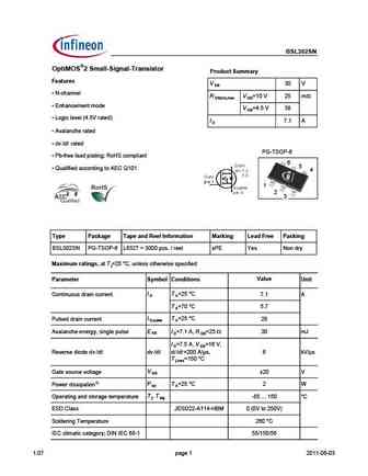
BSL302SN OptiMOS 2 Small-Signal-Transistor Product Summary Features V 30 V DS N-channel R V =10 V 25 m DS(on),max GS Enhancement mode V =4.5 V 38 GS Logic level (4.5V rated) I 7.1 A D Avalanche rated dv /dt rated PG-TSOP-6 Pb-free lead plating; RoHS compliant 6 5 Qualified according to AEC Q101 4 1 2 3 Type Package Tape and Reel Informa... See More ⇒
bsl308pe.pdf
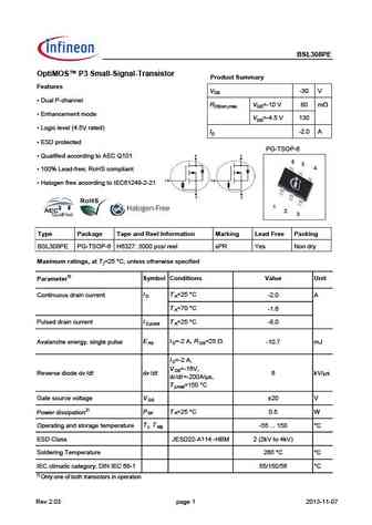
BSL308PE OptiMOS P3 Small-Signal-Transistor Product Summary Features VDS -30 V Dual P-channel RDS(on),max VGS=-10 V 80 mW Enhancement mode VGS=-4.5 V 130 Logic level (4.5V rated) ID -2.0 A ESD protected PG-TSOP-6 Qualified according to AEC Q101 6 5 4 100% Lead-free; RoHS compliant Halogen free according to IEC61249-2-21 1 2 3 Ty... See More ⇒
bsl306n.pdf
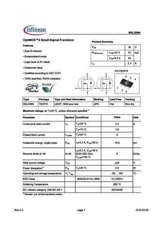
BSL306N $=@6"$'F ' .99 '64;.9 (>.;?6?@ %>E Features 0 V DS T H5@ ) 7... See More ⇒
bsl305spe.pdf

Mosfet Metal Oxide Semiconductor Field Effect Transistor OptiMOS Power-Transistor, -30V BSL305SPE Data Sheet Rev. 2.0 Final Industrial & Multimarket BSL305SPE OptiMOS -P 3 Small-Signal-Transistor Product Summary Features VDS -30 V P-channel RDS(on),max VGS=-10 V 45 m Enhancement mode VGS=-4.5 V 80 Logic level (4.5V rated) ID -5.3 A ESD protected ... See More ⇒
Detailed specifications: BSH111BK, BSH112, BSH205G2, BSL202SN, BSL205N, BSL207N, BSL214N, BSL215C, IRF630, BSL303SPE, BSL305SPE, BSL306N, BSL308C, BSL316C, BSL606SN, BSL802SN, BSL806N
Keywords - BSL302SN MOSFET specs
BSL302SN cross reference
BSL302SN equivalent finder
BSL302SN pdf lookup
BSL302SN substitution
BSL302SN replacement
Step-by-step guide to finding a MOSFET replacement. Cross-reference parts and ensure compatibility for your repair or project.
History: PSMN8R7-80BS
🌐 : EN ES РУ

LIST
Last Update
MOSFET: AUB062N08BG | AUB060N08AG | AUB056N10 | AUB056N08BGL | AUB050N085 | AUB050N055 | AUB045N12 | AUB045N10BT | AUB039N10 | AUB034N10
Popular searches
2sc733 | a933 transistor | d209l | irfb4321 | 2n333 | c3852 | irfp140 | ksc2383 datasheet