75N05E Specs and Replacement
Type Designator: 75N05E
Type of Transistor: MOSFET
Type of Control Channel: N-Channel
Absolute Maximum Ratings
Pd ⓘ - Maximum Power Dissipation: 240 W
|Vds|ⓘ - Maximum Drain-Source Voltage: 50 V
|Vgs|ⓘ - Maximum Gate-Source Voltage: 20 V
|Id| ⓘ - Maximum Drain Current: 75 A
Tj ⓘ - Maximum Junction Temperature: 175 °C
Electrical Characteristics
tr ⓘ - Rise Time: 75 nS
RDSonⓘ - Maximum Drain-Source On-State Resistance: 0.008 Ohm
Package: TO-3P
75N05E substitution
- MOSFET ⓘ Cross-Reference Search
75N05E datasheet
75n05e.pdf
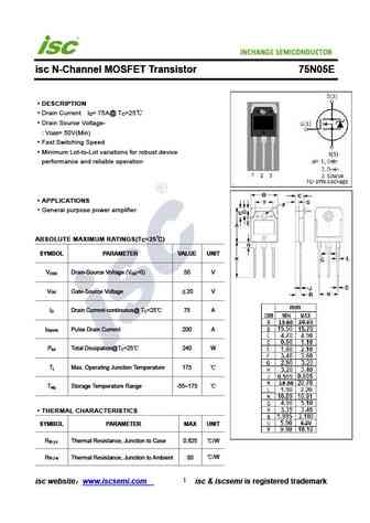
isc N-Channel MOSFET Transistor 75N05E DESCRIPTION Drain Current I = 75A@ T =25 D C Drain Source Voltage- V = 50V(Min) DSS Fast Switching Speed Minimum Lot-to-Lot variations for robust device performance and reliable operation APPLICATIONS General purpose power amplifier ABSOLUTE MAXIMUM RATINGS(T =25 ) C SYMBOL PARAMETER VALUE UNIT V Drain-Source Voltage (V ... See More ⇒
rfg75n05e.pdf
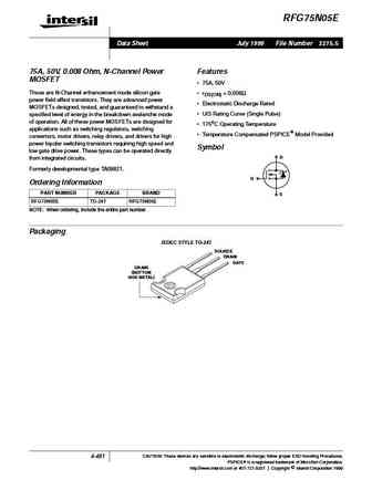
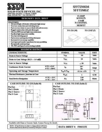
RFG75N05E Data Sheet July 1999 File Number 2275.5 75A, 50V, 0.008 Ohm, N-Channel Power Features MOSFET 75A, 50V These are N-Channel enhancement mode silicon gate rDS(ON) = 0.008 power field effect transistors. They are advanced power Electrostatic Discharge Rated MOSFETs designed, tested, and guaranteed to withstand a UIS Rating Curve (Single Pulse) specified level... See More ⇒
mtb75n05hd.pdf

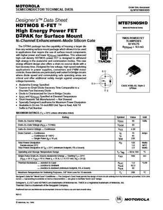
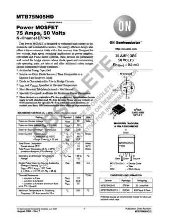
MOTOROLA Order this document SEMICONDUCTOR TECHNICAL DATA by MTB75N05HD/D Designer's Data Sheet MTB75N05HD HDTMOS E-FET. Motorola Preferred Device High Energy Power FET D2PAK for Surface Mount TMOS POWER FET 75 AMPERES N Channel Enhancement Mode Silicon Gate 50 VOLTS The D2PAK package has the capability of housing a larger die RDS(on) = 9.5 m than any existing sur... See More ⇒
mtp75n05hd.pdf
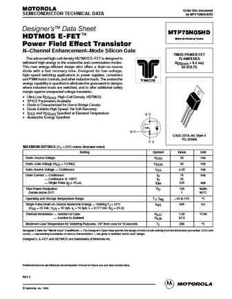
MOTOROLA Order this document SEMICONDUCTOR TECHNICAL DATA by MTP75N05HD/D Designer's Data Sheet MTP75N05HD HDTMOS E-FET Motorola Preferred Device Power Field Effect Transistor N Channel Enhancement Mode Silicon Gate TMOS POWER FET This advanced high cell density HDTMOS E FET is designed to 75 AMPERES withstand high energy in the avalanche and commutation modes. RDS... See More ⇒
Detailed specifications: 45N06, 45N20, RFM4N35, RFM4N40, 4N60AS, 50N06FI, 5NA80, 60N06-14, K2611, 8N90A, 9N80A, 9N90L-T3P, BUK444-200A, BUK444-800, BUK445-200B, BUK445-60H, BUK453-60B
Keywords - 75N05E MOSFET specs
75N05E cross reference
75N05E equivalent finder
75N05E pdf lookup
75N05E substitution
75N05E replacement
Can't find your MOSFET? Learn how to find a substitute transistor by analyzing voltage, current and package compatibility
History: CM2N65F | STM8362 | TK62N60X
🌐 : EN ES РУ

LIST
Last Update
MOSFET: AUB034N10 | AUB033N08BG | AUB026N085 | AUA062N08BG | AUA060N08AG | AUA056N08BGL | AUA039N10 | ASW80R290E | ASW65R120EFD | ASW65R110E
Popular searches
ncep039n10m | 20n50 | 2sc869 | tip29 transistor equivalent | 2n555 | 2sa564a | c815 transistor | ksa1381 equivalent