40N20 Specs and Replacement
Type Designator: 40N20
Type of Transistor: MOSFET
Type of Control Channel: N-Channel
Absolute Maximum Ratings
Pd ⓘ
- Maximum Power Dissipation: 220 W
|Vds|ⓘ - Maximum Drain-Source Voltage: 200 V
|Vgs|ⓘ - Maximum Gate-Source Voltage: 20 V
|Id| ⓘ - Maximum Drain Current: 40 A
Tj ⓘ - Maximum Junction Temperature: 175 °C
Electrical Characteristics
tr ⓘ - Rise Time: 24 nS
Cossⓘ -
Output Capacitance: 290 pF
RDSonⓘ - Maximum Drain-Source On-State Resistance: 0.05 Ohm
Package: TO220
- MOSFET ⓘ Cross-Reference Search
40N20 datasheet
..1. Size:213K inchange semiconductor
40n20.pdf 
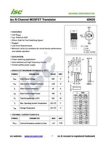
INCHANGE Semiconductor isc N-Channel MOSFET Transistor 40N20 FEATURES Low R DS(on) V Rated at 20V GS Silicon Gate for Fast Switching Speed Rugged Low Drive Requirements Minimum Lot-to-Lot variations for robust device performance and reliable operation DESCRITION Power switching applications Hard switched and high frequency circuits Uninterruptible power su... See More ⇒
0.1. Size:644K st
stf40n20.pdf

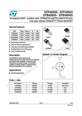
STP40N20-STF40N20 STB40N20 - STW40N20 N-CHANNEL 200V - 0.038 - 40A TO-220/FP/TO-247/D2PAK LOW GATE CHARGE STripFET MOSFET Table 1 General Features Figure 1 Package TYPE VDSS RDS(on) ID Pw STP40N20 200 V ... See More ⇒
0.5. Size:92K ixys
ixfn140n20p.pdf
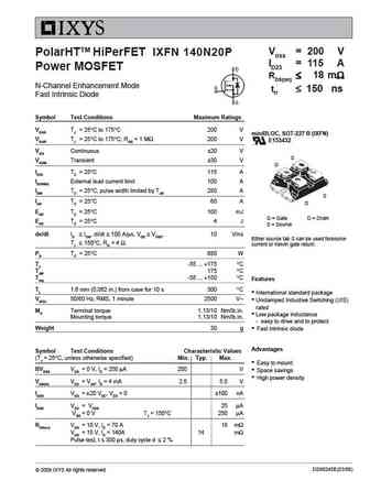
VDSS = 200 V IXFN 140N20P PolarHTTM HiPerFET ID25 = 115 A Power MOSFET RDS(on) 18 m N-Channel Enhancement Mode trr 150 ns Fast Intrinsic Diode Symbol Test Conditions Maximum Ratings VDSS TJ = 25 C to 175 C 200 V miniBLOC, SOT-227 B (IXFN) VDGR TJ = 25 C to 175 C; RGS = 1 M 200 V E153432 VGS Continuous 20 V S ... See More ⇒
0.6. Size:225K ixys
ixfk140n20p.pdf
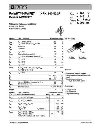
VDSS = 200 V IXFK 140N20P PolarHTTMHiPerFET ID25 = 140 A Power MOSFET RDS(on) 18 m trr 200 ns N-Channel Enhancement Mode Avalanche Rated Fast Intrinsic Diode Symbol Test Conditions Maximum Ratings TO-264 (IXFK) VDSS TJ = 25 C to 175 C 200 V VDGR TJ = 25 C to 175 C; RGS = 1 M 200 V VGS Continous 20 V V... See More ⇒
0.7. Size:162K ixys
ixtk140n20p.pdf
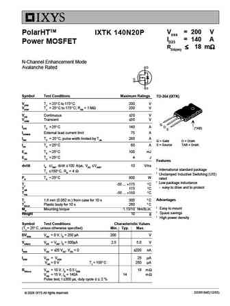
VDSS = 200 V IXTK 140N20P PolarHTTM ID25 = 140 A Power MOSFET RDS(on) 18 m N-Channel Enhancement Mode Avalanche Rated Symbol Test Conditions Maximum Ratings TO-264 (IXTK) VDSS TJ = 25 C to 175 C 200 V VDGR TJ = 25 C to 175 C; RGS = 1 M 200 V VGS Continuous 20 V VGSM Transient 30 V G ID25 TC = 25 C 140 A D (TAB) S ID(R... See More ⇒
0.8. Size:139K ixys
ixfr140n20p.pdf
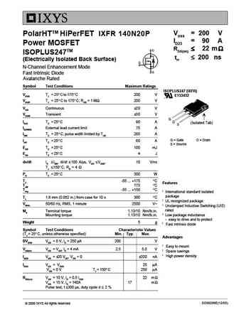
VDSS = 200 V IXFR 140N20P PolarHTTM HiPerFET ID25 = 90 A Power MOSFET RDS(on) 22 m ISOPLUS247TM trr 200 ns (Electrically Isolated Back Surface) N-Channel Enhancement Mode Fast Intrinsic Diode Avalanche Rated Symbol Test Conditions Maximum Ratings ISOPLUS247 (IXFR) VDSS TJ = 25 C to 175 C 200 V E153432 VDGR ... See More ⇒
0.9. Size:289K analog power
am40n20-180p.pdf
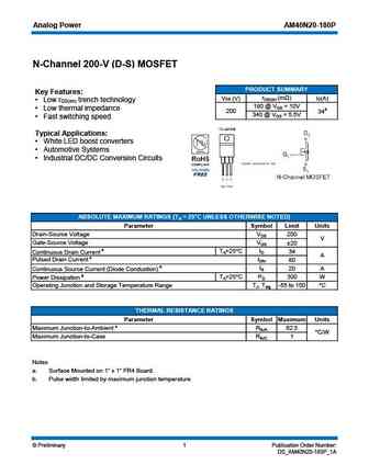
Analog Power AM40N20-180P N-Channel 200-V (D-S) MOSFET PRODUCT SUMMARY Key Features rDS(on) (m ) VDS (V) ID(A) Low r trench technology DS(on) 180 @ VGS = 10V Low thermal impedance 200 34a 340 @ VGS = 5.5V Fast switching speed Typical Applications White LED boost converters Automotive Systems Industrial DC/DC Conversion Circuits ABSOLUTE MAXIM... See More ⇒
0.10. Size:895K jilin sino
mt40n20a.pdf
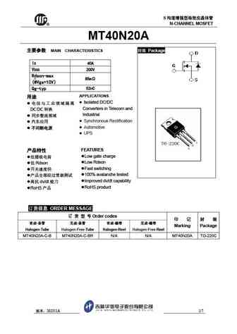
N N-CHANNEL MOSFET MT40N20A MAIN CHARACTERISTICS Package ID 40A VDSS 200V Rdson-max - 85m (@Vgs=10V Qg-typ 52nC APPLICATIONS Isolated DC/DC Converters in Telecom and DC/DC Industrial Synchronous Rectification ... See More ⇒
0.11. Size:549K cystek
mte040n20p3.pdf
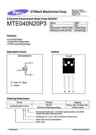
Spec. No. C872P3 Issued Date 2014.08.13 CYStech Electronics Corp. Revised Date Page No. 1/8 N-Channel Enhancement Mode Power MOSFET BVDSS 200V MTE040N20P3 ID 50A RDS(ON)@VGS=10V, ID=28A 30.2m (typ) RDS(ON)@VGS=6V, ID=10A 29.3m (typ) Features Low Gate Charge Simple Drive Requirement Pb-free lead plating package Equivalent Circuit Outline MT... See More ⇒
0.12. Size:1194K blue-rocket-elect
br40n20.pdf
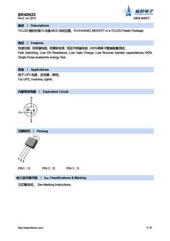
BR40N20 Rev.F Jul.-2018 DATA SHEET / Descriptions TO-220 N MOS N-CHANNEL MOSFET in a TO-220 Plastic Package. / Features , , , , 100 Fast Switching, Low ON Resistance, Low Gate Charge, Low Reverse transfer capacitances,100% Single Pulse... See More ⇒
0.13. Size:216K crhj
cs40n20 a8.pdf
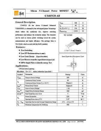
Silicon N-Channel Power MOSFET R CS40N20 A8 General Description VDSS 200 V CS40N20 A8 the silicon N-channel Enhanced ID 40 A PD (TC=25 ) 250 W VDMOSFETs, is obtained by the self-aligned planar Technology RDS(ON)Typ 0.054 which reduce the conduction loss, improve switching performance and enhance the avalanche energy. The transistor can be used in various po... See More ⇒
0.14. Size:233K crhj
cs40n20 anh.pdf
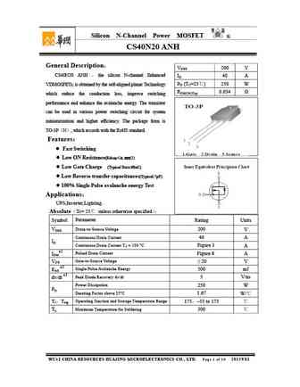
Silicon N-Channel Power MOSFET R CS40N20 ANH General Description VDSS 200 V CS40N20 ANH the silicon N-channel Enhanced ID 40 A PD (TC=25 ) 250 W VDMOSFETs, is obtained by the self-aligned planar Technology RDS(ON)Typ 0.054 which reduce the conduction loss, improve switching performance and enhance the avalanche energy. The transistor can be used in vario... See More ⇒
0.15. Size:222K crhj
cs40n20f a9h.pdf
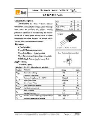
Silicon N-Channel Power MOSFET R CS40N20F A9H General Description VDSS 200 V CS40N20FA9H the silicon N-channel Enhanced ID 40 A PD (TC=25 ) 250 W VDMOSFETs, is obtained by the self-aligned planar Technology RDS(ON)Typ 0.054 which reduce the conduction loss, improve switching performance and enhance the avalanche energy. The transistor can be used in variou... See More ⇒
0.16. Size:216K crhj
cs40n20f a9e.pdf
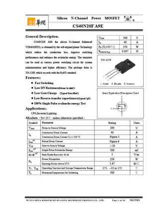
Silicon N-Channel Power MOSFET R CS40N20F A9E General Description VDSS 200 V CS40N20F A9E the silicon N-channel Enhanced ID 40 A PD (TC=25 ) 250 W VDMOSFETs, is obtained by the self-aligned planar Technology RDS(ON)Typ 0.047 which reduce the conduction loss, improve switching performance and enhance the avalanche energy. The transistor can be used in vari... See More ⇒
0.17. Size:124K jdsemi
cm40n20 to220.pdf
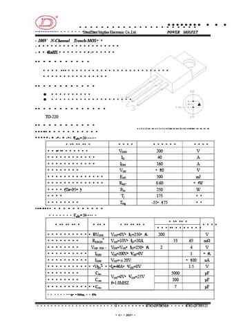
R CM40N20 www.jdsemi.cn ShenZhen Jingdao Electronic Co.,Ltd. POWER MOSFET 200V N-Channel Trench-MOS RoHS 1 US P 2 3 ... See More ⇒
0.18. Size:1195K feihonltd
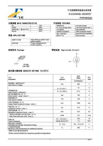
fhp40n20c.pdf

N N-CHANNEL MOSFET FHP40N20C MAIN CHARACTERISTICS FEATURES ID 40A Low gate charge VDSS 200V Crss ( 34pF) Low Crss (typical 34pF ) Rdson-typ @Vgs=10V 50m Fast switching Qg-typ 49.4nC 100% 100% avalanche tested dv/dt Improved dv/... See More ⇒
0.19. Size:1114K feihonltd
fhp40n20a.pdf
N N-CHANNEL MOSFET FHP40N20A MAIN CHARACTERISTICS FEATURES ID 35A Low gate charge VDSS 200V Crss ( 24pF) Low Crss (typical 24pF ) Rdson-typ @Vgs=10V 70m Fast switching Qg-typ 38nC 100% 100% avalanche tested dv/dt Improved dv/dt... See More ⇒
0.20. Size:836K pipsemi
ptp40n20.pdf
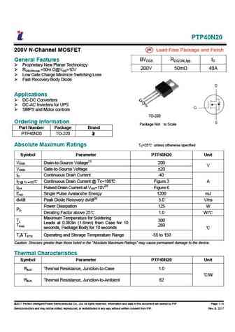
PTP40N20 200V N-Channel MOSFET General Features BVDSS RDS(ON),typ. ID Proprietary New Planar Technology 200V 50m 40A RDS(ON),typ.=50m @VGS=10V Low Gate Charge Minimize Switching Loss Fast Recovery Body Diode Applications DC-DC Converters G D S DC-AC Inverters for UPS SMPS and Motor controls TO-220 Ordering Information Package Not... See More ⇒
0.21. Size:23K shaanxi
wvm40n20.pdf

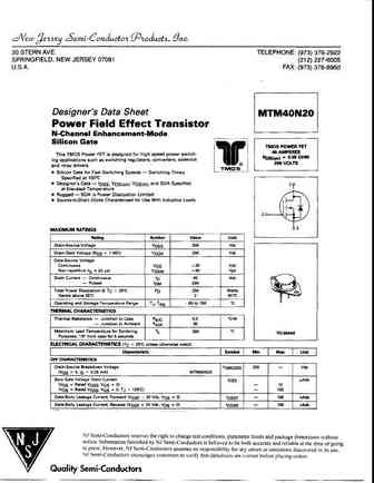
Shaanxi Qunli Electric Co., Ltd Add. No. 1 Qunli Road,Baoji City,Shaanxi,China WVM40N20(MTM40N20) Power MOSFET(N-channel) Transistor Features 1. It s voltage control component with good input impedance, small starting power dissipation, wide area of safe operation, good temperature stability. 2. Implementation of standards QZJ840611 3. Use for high speed switch, circuit of powe... See More ⇒
0.22. Size:1115K way-on
wmb340n20hg2.pdf
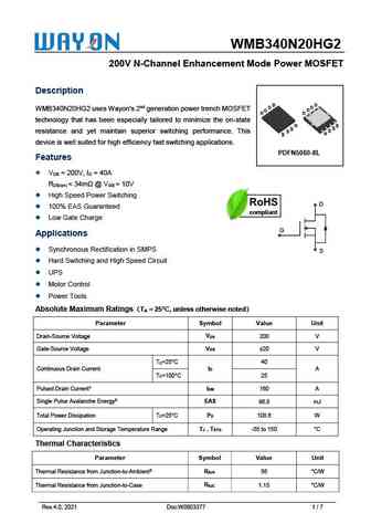
WMB340N20HG2 200V N-Channel Enhancement Mode Power MOSFET Description D D D WMB340N20HG2 uses Wayon's 2nd generation power trench MOSFET DD D D D technology that has been especially tailored to minimize the on-state G ss resistance and yet maintain superior switching performance. This s ss G s device is well suited for high efficiency fast switching applications. PDFN5060... See More ⇒
0.23. Size:540K way-on
wml340n20hg2.pdf
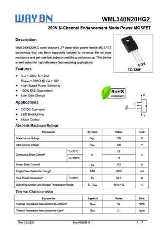
WML340N20HG2 200V N-Channel Enhancement Mode Power MOSFET Description WML340N20HG2 uses Wayon's 2nd generation power trench MOSFET technology that has been especially tailored to minimize the on-state resistance and yet maintain superior switching performance. This device is well suited for high efficiency fast switching applications. GDS Features TO-220F V = 200V, I = 28A... See More ⇒
0.24. Size:521K way-on
wmm340n20hg2.pdf
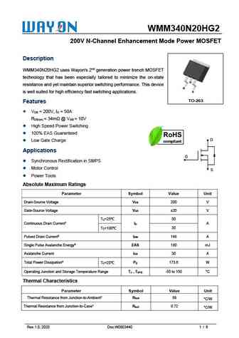
WMM340N20HG2 200V N-Channel Enhancement Mode Power MOSFET Description WMM340N20HG2 uses Wayon's 2nd generation power trench MOSFET technology that has been especially tailored to minimize the on-state D resistance and yet maintain superior switching performance. This device G is well suited for high efficiency fast switching applications. S TO-263 Features V = 200V, I = 50... See More ⇒
0.25. Size:471K way-on
wmk340n20hg2.pdf
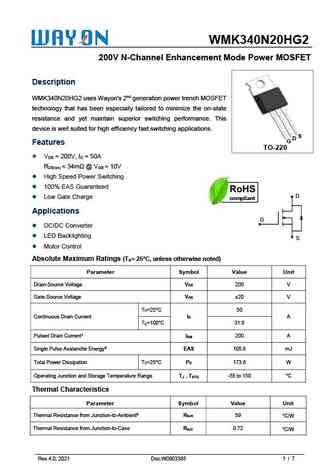
WMK340N20HG2 200V N-Channel Enhancement Mode Power MOSFET Description WMK340N20HG2 uses Wayon's 2nd generation power trench MOSFET technology that has been especially tailored to minimize the on-state resistance and yet maintain superior switching performance. This device is well suited for high efficiency fast switching applications. S D G Features TO-220 V = 200V, I = ... See More ⇒
0.26. Size:216K wuxi china
cs40n20a8.pdf

Silicon N-Channel Power MOSFET R CS40N20 A8 General Description VDSS 200 V CS40N20 A8 the silicon N-channel Enhanced ID 40 A PD (TC=25 ) 250 W VDMOSFETs, is obtained by the self-aligned planar Technology RDS(ON)Typ 0.054 which reduce the conduction loss, improve switching performance and enhance the avalanche energy. The transistor can be used in various po... See More ⇒
0.27. Size:800K convert
cs40n20f cs40n20p.pdf
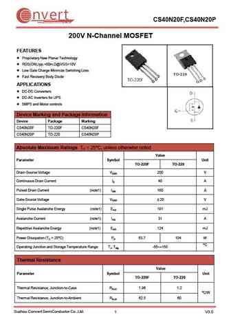
nvert CS40N20F,CS40N20P Suzhou Convert Semiconductor Co ., Ltd. 200V N-Channel MOSFET FEATURES Proprietary New Planar Technology RDS(ON),typ.=50m @VGS=10V Low Gate Charge Minimize Switching Loss Fast Recovery Body Diode APPLICATIONS DC-DC Converters DC-AC Inverters for UPS SMPS and Motor controls Device Marking and Package Information Device Package ... See More ⇒
0.28. Size:4328K first semi
fir40n20lg.pdf

FIR40N20LG N-Channel Enhancement Mode Power Mosfet PIN Connection TO-252 Description The FIR40N20LG uses advanced trench technology and design to provide excellent RDS(ON) with low gate charge. It can be used in a wide variety of applications. General Features VDS =200V,ID =24A RDS(ON) ... See More ⇒
0.29. Size:512K cn hmsemi
hm40n20.pdf
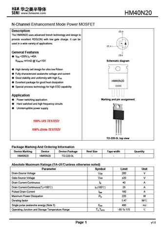
HM40N20 N-Channel Enhancement Mode Power MOSFET Description The HM40N20 uses advanced trench technology and design to provide excellent RDS(ON) with low gate charge. It can be used in a wide variety of applications. General Features VDS =200V,ID =40A RDS(ON) ... See More ⇒
0.30. Size:599K cn hmsemi
hm40n20d.pdf
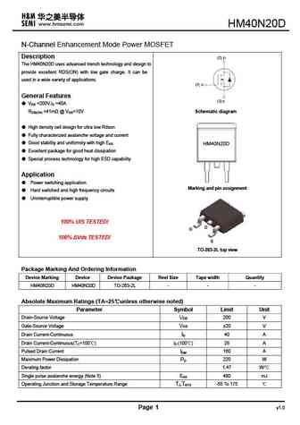
HM40N20D N-Channel Enhancement Mode Power MOSFET Description The HM40N20D uses advanced trench technology and design to provide excellent RDS(ON) with low gate charge. It can be used in a wide variety of applications. General Features VDS =200V,ID =40A RDS(ON) ... See More ⇒
0.31. Size:576K cn minos
mp40n20.pdf
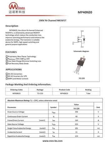
200V N-Channel MOSFET Description MP40N20, the silicon N-channel Enhanced MOSFETs, is obtained by advanced MOSFET technology which reduce the conduction loss, improve switching performance and enhance the avalanche energy. The transistor is suitable device for SMPS, high speed switching and general purpose applications Schematic diagram FEATURES Proprietary New Planar Technology ... See More ⇒
0.32. Size:797K cn fx-semi
fxn40n20c.pdf
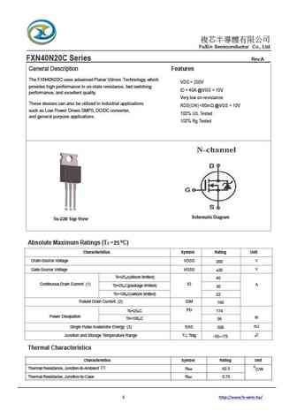
FuXin Semiconductor Co., Ltd. FXN40N20C Series Rev.A General Description Features The FXN40N20C uses advanced Planar Vdmos Technology, which VDS = 200V provides high performance in on-state resistance, fast switching ID = 40A @VGS = 10V performance, and excellent quality. Very low on-resistance These devices can also be utilized in industrial applications ... See More ⇒
0.33. Size:2811K cn apm
ap40n20mp.pdf
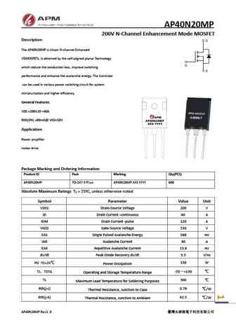
AP40N20MP 200V N-Channel Enhancement Mode MOSFET Description The AP40N20MP is silicon N-channel Enhanced VDMOSFETs, is obtained by the self-aligned planar Technology which reduce the conduction loss, improve switching performance and enhance the avalanche energy. The transistor can be used in various power switching circuit for system miniaturization and higher efficiency. G... See More ⇒
0.34. Size:1423K cn apm
ap40n20p ap40n20t.pdf

AP40N20PIT 200V N-Channel Enhancement Mode MOSFET Description The AP40N20P/T is silicon N-channel Enhanced VDMOSFETs, is obtained by the self-aligned planar Technology which reduce the conduction loss, improve switching performance and enhance the avalanche energy. The transistor can be used in various power switching circuit for system miniaturization and higher efficiency. ... See More ⇒
Detailed specifications: 2SK754
, 2SK755
, 2SK756
, 2SK757
, 2SK759
, 2SK763
, 2SK766
, 2SK767
, 2N7000
, FIR4N65F
, IRFP256
, IRFP257
, SUD40N06-25L
, DTU40N06
, SUP40N06-25L
, SUB40N06-25L
, BR80N08A
.
Keywords - 40N20 MOSFET specs
40N20 cross reference
40N20 equivalent finder
40N20 pdf lookup
40N20 substitution
40N20 replacement
Can't find your MOSFET?
Learn how to find a substitute transistor by analyzing voltage, current and package compatibility