NDP608BE Datasheet. Specs and Replacement
Type Designator: NDP608BE
Type of Transistor: MOSFET
Type of Control Channel: N-Channel
Absolute Maximum Ratings
Pd ⓘ - Maximum Power Dissipation: 100 W
|Vds|ⓘ - Maximum Drain-Source Voltage: 80 V
|Vgs|ⓘ - Maximum Gate-Source Voltage: 20 V
|Id| ⓘ - Maximum Drain Current: 32 A
Tj ⓘ - Maximum Junction Temperature: 175 °C
Electrical Characteristics
tr ⓘ - Rise Time: 113 nS
Cossⓘ - Output Capacitance: 390 pF
RDSonⓘ - Maximum Drain-Source On-State Resistance: 0.045 Ohm
Package: TO-220
NDP608BE substitution
- MOSFET ⓘ Cross-Reference Search
NDP608BE datasheet
ndb608ae ndb608b ndb608be ndp608ae ndp608b ndp608be.pdf
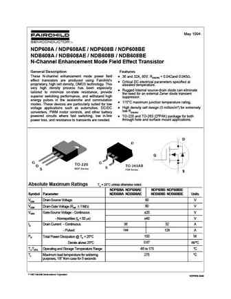
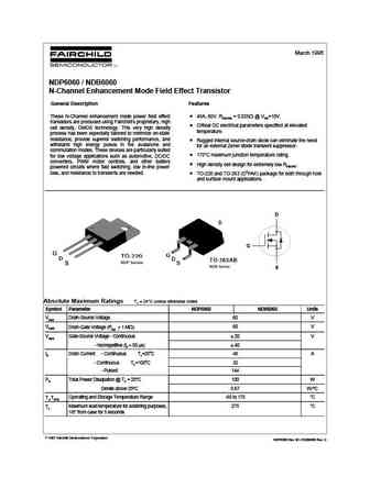
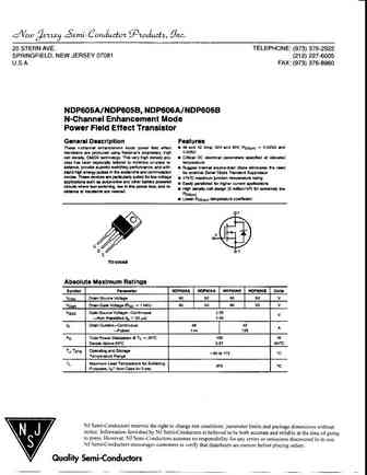
May 1994 NDP608A / NDP608AE / NDP608B / NDP608BE NDB608A / NDB608AE / NDB608B / NDB608BE N-Channel Enhancement Mode Field Effect Transistor General Description Features These N-channel enhancement mode power field 36 and 32A, 80V. RDS(ON) = 0.042and 0.045 . effect transistors are produced using Fairchild's Critical DC electrical parameters specified at proprietary, high cell densi... See More ⇒
ndp6030pl ndb6030pl.pdf
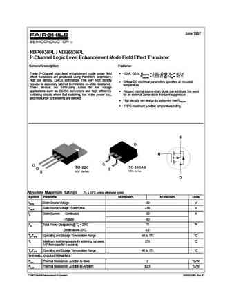
June 1997 NDP6030PL / NDB6030PL P-Channel Logic Level Enhancement Mode Field Effect Transistor General Description Features These P-Channel logic level enhancement mode power field -30 A, -30 V. RDS(ON) = 0.042 @ VGS= -4.5 V RDS(ON) = 0.025 @ VGS= -10 V. effect transistors are produced using Fairchild's proprietary, high cell density, DMOS technology. This very high density ... See More ⇒
ndp6060l ndb6060l.pdf
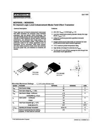
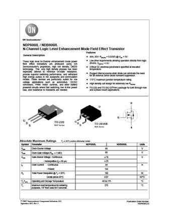
April 1996 NDP6060L / NDB6060L N-Channel Logic Level Enhancement Mode Field Effect Transistor General Description Features 48A, 60V. RDS(ON) = 0.025 @ VGS = 5V. These logic level N-Channel enhancement mode power field effect transistors are produced using Fairchild's Low drive requirements allowing operation directly from logic proprietary, high cell density, DMOS technology. This... See More ⇒
ndp6020p ndb6020p.pdf
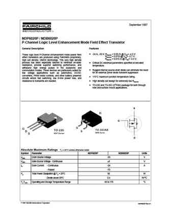
September 1997 NDP6020P / NDB6020P P-Channel Logic Level Enhancement Mode Field Effect Transistor General Description Features -24 A, -20 V. RDS(ON) = 0.05 @ VGS= -4.5 V. These logic level P-Channel enhancement mode power field RDS(ON) = 0.07 @ VGS= -2.7 V. effect transistors are produced using Fairchild's proprietary, RDS(ON) = 0.075 @ VGS= -2.5 V. high cell density,... See More ⇒
Detailed specifications: NDP410B, NDP410BE, NDP605A, NDP605B, NDP606A, NDP606B, NDP608AE, NDP608B, STF13NM60N, NDP610AE, NDP610B, NDP610BE, NDP708AE, NDP708B, NDP708BE, NDP710AE, NDP710B
Keywords - NDP608BE MOSFET specs
NDP608BE cross reference
NDP608BE equivalent finder
NDP608BE pdf lookup
NDP608BE substitution
NDP608BE replacement
Learn how to find the right MOSFET substitute. A guide to cross-reference, check specs and replace MOSFETs in your circuits.
History: IPP60R090CFD7 | RJK0303DPB
🌐 : EN ES РУ
LIST
Last Update
MOSFET: ASDM40N60KQ | ASDM40N40E | ASDM40N100P | ASDM40DN20E | ASDM3416EZA | ASDM3415ZA | ASDM3401ZA | ASDM3401 | ASDM3400ZA | ASDM30P30BE
Popular searches
mosfet k8a50d | sl100 transistor | d2499 datasheet | 6r190p6 datasheet | 2n270 | 2n2924 | mpsa65 | 2sa794
