NTMFS4C55N Datasheet. Specs and Replacement
Type Designator: NTMFS4C55N 📄📄
Type of Transistor: MOSFET
Type of Control Channel: N-Channel
Absolute Maximum Ratings
Pd ⓘ - Maximum Power Dissipation: 2.57 W
|Vds|ⓘ - Maximum Drain-Source Voltage: 30 V
|Vgs|ⓘ - Maximum Gate-Source Voltage: 20 V
|Id| ⓘ - Maximum Drain Current: 21.7 A
Tj ⓘ - Maximum Junction Temperature: 150 °C
Electrical Characteristics
tr ⓘ - Rise Time: 32 nS
Cossⓘ - Output Capacitance: 1215 pF
RDSonⓘ - Maximum Drain-Source On-State Resistance: 0.0034 Ohm
Package: SO-8
📄📄 Copy
- MOSFET ⓘ Cross-Reference Search
NTMFS4C55N datasheet
..1. Size:79K 1
ntmfs4c55n.pdf 
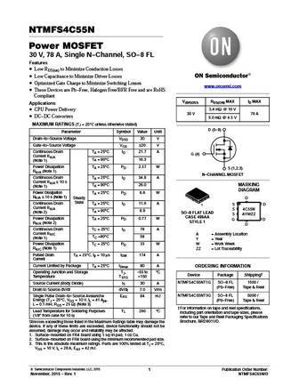
NTMFS4C55N Power MOSFET 30 V, 78 A, Single N-Channel, SO-8 FL Features Low RDS(on) to Minimize Conduction Losses Low Capacitance to Minimize Driver Losses Optimized Gate Charge to Minimize Switching Losses www.onsemi.com These Devices are Pb-Free, Halogen Free/BFR Free and are RoHS Compliant V(BR)DSS RDS(ON) MAX ID MAX Applications 3.4 mW @ 10 V CPU Power Delive... See More ⇒
..2. Size:79K onsemi
ntmfs4c55n.pdf
NTMFS4C55N Power MOSFET 30 V, 78 A, Single N-Channel, SO-8 FL Features Low RDS(on) to Minimize Conduction Losses Low Capacitance to Minimize Driver Losses Optimized Gate Charge to Minimize Switching Losses www.onsemi.com These Devices are Pb-Free, Halogen Free/BFR Free and are RoHS Compliant V(BR)DSS RDS(ON) MAX ID MAX Applications 3.4 mW @ 10 V CPU Power Delive... See More ⇒
6.1. Size:124K onsemi
ntmfs4c59n.pdf
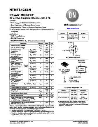
NTMFS4C59N Power MOSFET 30 V, 52 A, Single N-Channel, SO-8 FL Features Low RDS(on) to Minimize Conduction Losses Low Capacitance to Minimize Driver Losses http //onsemi.com Optimized Gate Charge to Minimize Switching Losses These Devices are Pb-Free and are RoHS Compliant V(BR)DSS RDS(ON) MAX ID MAX Applications 5.8 mW @ 10 V CPU Power Delivery 30 V 52 A 8.5 mW... See More ⇒
7.1. Size:138K 1
ntmfs4c06n.pdf
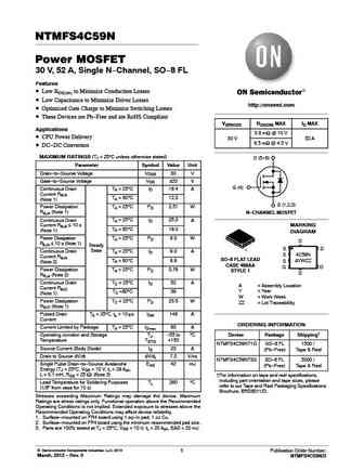
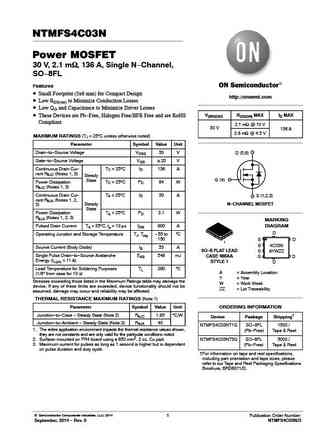
NTMFS4C06N MOSFET Power, Single, N-Channel, SO-8 FL 30 V, 69 A Features www.onsemi.com Low RDS(on) to Minimize Conduction Losses Low Capacitance to Minimize Driver Losses Optimized Gate Charge to Minimize Switching Losses V(BR)DSS RDS(ON) MAX ID MAX These Devices are Pb-Free, Halogen Free/BFR Free and are RoHS 4.0 mW @ 10 V Compliant 30 V 69 A 6.0 mW @ 4.5 V A... See More ⇒
7.2. Size:79K 1
ntmfs4c05nt1g.pdf
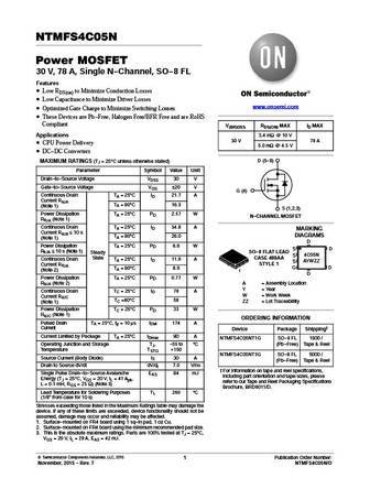
NTMFS4C05N Power MOSFET 30 V, 78 A, Single N-Channel, SO-8 FL Features Low RDS(on) to Minimize Conduction Losses Low Capacitance to Minimize Driver Losses www.onsemi.com Optimized Gate Charge to Minimize Switching Losses These Devices are Pb-Free, Halogen Free/BFR Free and are RoHS Compliant V(BR)DSS RDS(ON) MAX ID MAX Applications 3.4 mW @ 10 V 30 V 78 A CPU P... See More ⇒
7.3. Size:179K onsemi
ntmfs4c054n.pdf
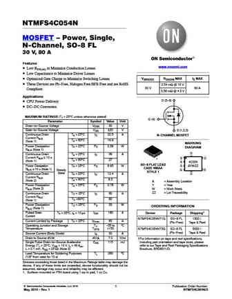
NTMFS4C054N MOSFET Power, Single, N-Channel, SO-8 FL 30 V, 80 A Features www.onsemi.com Low RDS(on) to Minimize Conduction Losses Low Capacitance to Minimize Driver Losses V(BR)DSS RDS(ON) MAX ID MAX Optimized Gate Charge to Minimize Switching Losses These Devices are Pb-Free, Halogen Free/BFR Free and are RoHS 2.54 mW @ 10 V 30 V 80 A Compliant 3.56 mW @ 4.5 V... See More ⇒
7.4. Size:173K onsemi
ntmfs4c022n.pdf
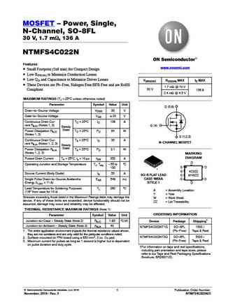
MOSFET Power, Single, N-Channel, SO-8FL 30 V, 1.7 mW, 136 A NTMFS4C022N Features www.onsemi.com Small Footprint (5x6 mm) for Compact Design Low RDS(on) to Minimize Conduction Losses Low QG and Capacitance to Minimize Driver Losses V(BR)DSS RDS(ON) MAX ID MAX These Devices are Pb-Free, Halogen Free/BFR Free and are RoHS 1.7 mW @ 10 V 30 V Compliant 136 A 2.4 mW... See More ⇒
7.5. Size:177K onsemi
ntmfs4c029n.pdf
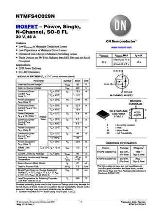
NTMFS4C029N MOSFET Power, Single, N-Channel, SO-8 FL 30 V, 46 A Features Low RDS(on) to Minimize Conduction Losses www.onsemi.com Low Capacitance to Minimize Driver Losses Optimized Gate Charge to Minimize Switching Losses V(BR)DSS RDS(ON) MAX ID MAX These Devices are Pb-Free, Halogen Free/BFR Free and are RoHS 5.88 mW @ 10 V Compliant 30 V 46 A 9.0 mW @ 4.5 V ... See More ⇒
7.6. Size:84K onsemi
ntmfs4c05n.pdf

NTMFS4C05N Power MOSFET 30 V, 78 A, Single N-Channel, SO-8 FL Features Low RDS(on) to Minimize Conduction Losses Low Capacitance to Minimize Driver Losses www.onsemi.com Optimized Gate Charge to Minimize Switching Losses These Devices are Pb-Free, Halogen Free/BFR Free and are RoHS Compliant V(BR)DSS RDS(ON) MAX ID MAX Applications 3.4 mW @ 10 V 30 V 78 A CPU P... See More ⇒
7.7. Size:88K onsemi
ntmfs4c10n.pdf

NTMFS4C10N Power MOSFET 30 V, 46 A, Single N-Channel, SO-8 FL Features Low RDS(on) to Minimize Conduction Losses Low Capacitance to Minimize Driver Losses Optimized Gate Charge to Minimize Switching Losses www.onsemi.com These Devices are Pb-Free, Halogen Free/BFR Free and are RoHS Compliant V(BR)DSS RDS(ON) MAX ID MAX Applications 6.95 mW @ 10 V CPU Power Delive... See More ⇒
7.8. Size:175K onsemi
ntmfs4c020n.pdf
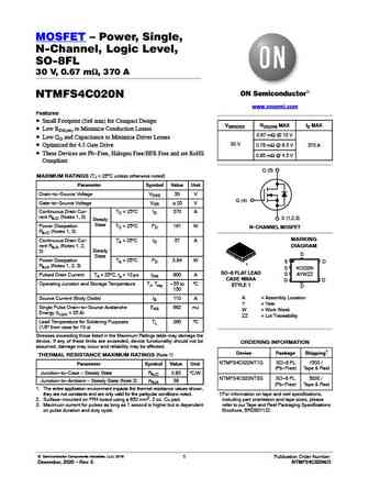
MOSFET Power, Single, N-Channel, Logic Level, SO-8FL 30 V, 0.67 mW, 370 A NTMFS4C020N www.onsemi.com Features Small Footprint (5x6 mm) for Compact Design V(BR)DSS RDS(ON) MAX ID MAX Low RDS(on) to Minimize Conduction Losses 0.67 mW @ 10 V Low QG and Capacitance to Minimize Driver Losses 30 V 0.78 mW @ 6.5 V 370 A Optimized for 4.5 Gate Drive These Devices ... See More ⇒
7.9. Size:93K onsemi
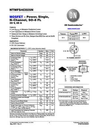
ntmfs4c09nt1g.pdf

NTMFS4C09N Power MOSFET 30 V, 52 A, Single N-Channel, SO-8 FL Features Low RDS(on) to Minimize Conduction Losses Low Capacitance to Minimize Driver Losses www.onsemi.com Optimized Gate Charge to Minimize Switching Losses These Devices are Pb-Free, Halogen Free/BFR Free and are RoHS V(BR)DSS RDS(ON) MAX ID MAX Compliant 5.8 mW @ 10 V Applications 30 V 52 A 8.5 mW @ ... See More ⇒
7.10. Size:115K onsemi
ntmfs4c03n.pdf
NTMFS4C03N Power MOSFET 30 V, 2.1 mW, 136 A, Single N-Channel, SO-8FL Features Small Footprint (5x6 mm) for Compact Design http //onsemi.com Low RDS(on) to Minimize Conduction Losses Low QG and Capacitance to Minimize Driver Losses V(BR)DSS RDS(ON) MAX ID MAX These Devices are Pb-Free, Halogen Free/BFR Free and are RoHS Compliant 2.1 mW @ 10 V 30 V 136 A 2.8 mW @ ... See More ⇒
7.11. Size:116K onsemi
ntmfs4c13n.pdf
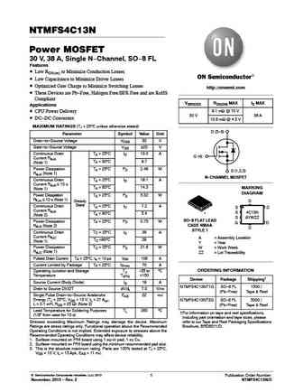
NTMFS4C13N Power MOSFET 30 V, 38 A, Single N-Channel, SO-8 FL Features Low RDS(on) to Minimize Conduction Losses Low Capacitance to Minimize Driver Losses Optimized Gate Charge to Minimize Switching Losses http //onsemi.com These Devices are Pb-Free, Halogen Free/BFR Free and are RoHS Compliant V(BR)DSS RDS(ON) MAX ID MAX Applications 9.1 mW @ 10 V CPU Power Del... See More ⇒
7.12. Size:91K onsemi
ntmfs4c08n.pdf
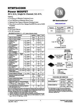
NTMFS4C08N Power MOSFET 30 V, 52 A, Single N-Channel, SO-8 FL Features Low RDS(on) to Minimize Conduction Losses Low Capacitance to Minimize Driver Losses Optimized Gate Charge to Minimize Switching Losses www.onsemi.com These Devices are Pb-Free, Halogen Free/BFR Free and are RoHS Compliant Applications V(BR)DSS RDS(ON) MAX ID MAX CPU Power Delivery 5.8 mW @ 10 ... See More ⇒
7.13. Size:117K onsemi
ntmfs4c35n.pdf
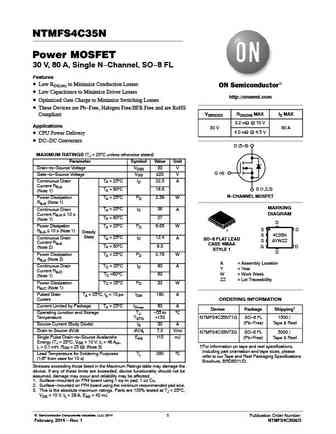
NTMFS4C35N Power MOSFET 30 V, 80 A, Single N-Channel, SO-8 FL Features Low RDS(on) to Minimize Conduction Losses Low Capacitance to Minimize Driver Losses http //onsemi.com Optimized Gate Charge to Minimize Switching Losses These Devices are Pb-Free, Halogen Free/BFR Free and are RoHS V(BR)DSS RDS(ON) MAX ID MAX Compliant 3.2 mW @ 10 V Applications 30 V 80 A 4.0 mW... See More ⇒
7.14. Size:139K onsemi
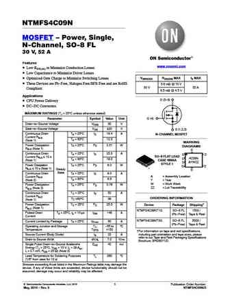
ntmfs4c025n.pdf
NTMFS4C025N MOSFET Power, Single, N-Channel, SO-8 FL 30 V, 69 A Features www.onsemi.com Low RDS(on) to Minimize Conduction Losses Low Capacitance to Minimize Driver Losses V(BR)DSS RDS(ON) MAX ID MAX Optimized Gate Charge to Minimize Switching Losses These Devices are Pb-Free, Halogen Free/BFR Free and are RoHS 3.41 mW @ 10 V 30 V 69 A Compliant 4.88 mW @ 4.5 V ... See More ⇒
7.15. Size:140K onsemi
ntmfs4c09n.pdf
NTMFS4C09N MOSFET Power, Single, N-Channel, SO-8 FL 30 V, 52 A Features www.onsemi.com Low RDS(on) to Minimize Conduction Losses Low Capacitance to Minimize Driver Losses V(BR)DSS RDS(ON) MAX ID MAX Optimized Gate Charge to Minimize Switching Losses These Devices are Pb-Free, Halogen Free/BFR Free and are RoHS 5.8 mW @ 10 V 30 V 52 A Compliant 8.5 mW @ 4.5 V A... See More ⇒
7.16. Size:182K onsemi
ntmfs4c250n.pdf
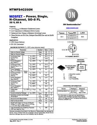
NTMFS4C250N MOSFET Power, Single, N-Channel, SO-8 FL 30 V, 69 A Features www.onsemi.com Low RDS(on) to Minimize Conduction Losses Low Capacitance to Minimize Driver Losses V(BR)DSS RDS(ON) MAX ID MAX Optimized Gate Charge to Minimize Switching Losses These Devices are Pb-Free, Halogen Free/BFR Free and are RoHS 4.0 mW @ 10 V 30 V 69 A Compliant 6.0 mW @ 4.5 V A... See More ⇒
7.17. Size:171K onsemi
ntmfs4c032n.pdf
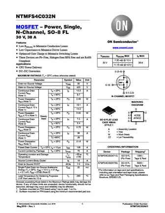
NTMFS4C032N MOSFET Power, Single, N-Channel, SO-8 FL 30 V, 38 A Features Low RDS(on) to Minimize Conduction Losses www.onsemi.com Low Capacitance to Minimize Driver Losses Optimized Gate Charge to Minimize Switching Losses V(BR)DSS RDS(ON) MAX ID MAX These Devices are Pb-Free, Halogen Free/BFR Free and are RoHS 7.35 mW @ 10 V Compliant 30 V 38 A Applications 1... See More ⇒
7.18. Size:178K onsemi
ntmfs4c027n.pdf
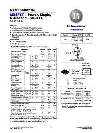
NTMFS4C027N MOSFET Power, Single, N-Channel, SO-8 FL 30 V, 52 A Features Low RDS(on) to Minimize Conduction Losses www.onsemi.com Low Capacitance to Minimize Driver Losses Optimized Gate Charge to Minimize Switching Losses These Devices are Pb-Free, Halogen Free/BFR Free and are RoHS V(BR)DSS RDS(ON) MAX ID MAX Compliant 4.8 mW @ 10 V 30 V 52 A Applications 7.4... See More ⇒
7.19. Size:93K onsemi
ntmfs4c06n.pdf
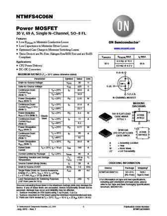
NTMFS4C06N Power MOSFET 30 V, 69 A, Single N-Channel, SO-8 FL Features Low RDS(on) to Minimize Conduction Losses Low Capacitance to Minimize Driver Losses www.onsemi.com Optimized Gate Charge to Minimize Switching Losses These Devices are Pb-Free, Halogen Free/BFR Free and are RoHS V(BR)DSS RDS(ON) MAX ID MAX Compliant 4.0 mW @ 10 V Applications 30 V 69 A CPU P... See More ⇒
7.20. Size:113K onsemi
ntmfs4c01n.pdf
NTMFS4C01N Power MOSFET 30 V, 0.9 mW, 303 A, Single N-Channel, SO-8FL Features Small Footprint (5x6 mm) for Compact Design http //onsemi.com Low RDS(on) to Minimize Conduction Losses Low QG and Capacitance to Minimize Driver Losses V(BR)DSS RDS(ON) MAX ID MAX These Devices are Pb-Free, Halogen Free/BFR Free and are RoHS Compliant 0.9 mW @ 10 V 30 V 303 A 1.2 mW @ ... See More ⇒
7.21. Size:182K onsemi
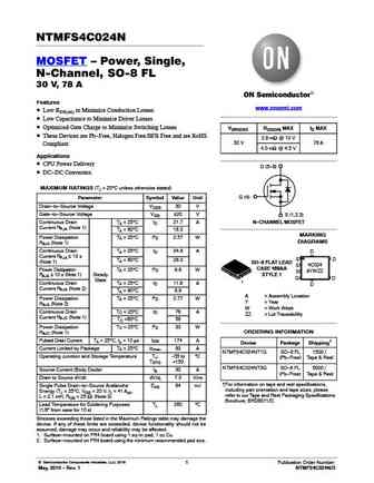
ntmfs4c028n.pdf
NTMFS4C028N MOSFET Power, Single, N-Channel, SO-8 FL 30 V, 52 A Features www.onsemi.com Low RDS(on) to Minimize Conduction Losses Low Capacitance to Minimize Driver Losses V(BR)DSS RDS(ON) MAX ID MAX Optimized Gate Charge to Minimize Switching Losses These Devices are Pb-Free, Halogen Free/BFR Free and are RoHS 4.73 mW @ 10 V 30 V 52 A Compliant 7.0 mW @ 4.5 V ... See More ⇒
7.22. Size:173K onsemi
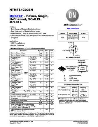
ntmfs4c024n.pdf
NTMFS4C024N MOSFET Power, Single, N-Channel, SO-8 FL 30 V, 78 A Features www.onsemi.com Low RDS(on) to Minimize Conduction Losses Low Capacitance to Minimize Driver Losses Optimized Gate Charge to Minimize Switching Losses V(BR)DSS RDS(ON) MAX ID MAX These Devices are Pb-Free, Halogen Free/BFR Free and are RoHS 2.8 mW @ 10 V 30 V 78 A Compliant 4.0 mW @ 4.5 V ... See More ⇒
7.23. Size:133K onsemi
ntmfs4c302n.pdf
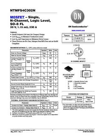
NTMFS4C302N MOSFET Single, N-Channel, Logic Level, SO-8 FL 30 V, 1.15 mW, 230 A www.onsemi.com Features Small Footprint (5x6 mm) for Compact Design V(BR)DSS RDS(on) MAX ID MAX Low RDS(on) to Minimize Conduction Losses 1.15 mW @ 10 V Low QG and Capacitance to Minimize Driver Losses 30 V 230 A 1.7 mW @ 4.5 V These Devices are Pb-Free, Halogen Free/BFR Free and a... See More ⇒
7.24. Size:177K onsemi
ntmfs4c290n.pdf
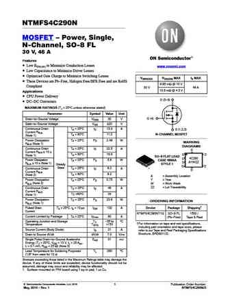
NTMFS4C290N MOSFET Power, Single, N-Channel, SO-8 FL 30 V, 46 A Features Low RDS(on) to Minimize Conduction Losses www.onsemi.com Low Capacitance to Minimize Driver Losses Optimized Gate Charge to Minimize Switching Losses V(BR)DSS RDS(ON) MAX ID MAX These Devices are Pb-Free, Halogen Free/BFR Free and are RoHS 6.95 mW @ 10 V Compliant 30 V 46 A 10.8 mW @ 4.5 V... See More ⇒
Detailed specifications: FTP50N20R, JCS12N65T, JCS12N65CT, JCS12N65FT, ME4410A, MMD65R600QRH, MT3245, NCE0117K, IRF3710, SI9953DY, STP110N7F6, SUP85N03-07P, SUB85N03-07P, SVF4N60CAF, SVF4N60CAK, SVF4N60CAD, SVF4N60CAT
Keywords - NTMFS4C55N MOSFET specs
NTMFS4C55N cross reference
NTMFS4C55N equivalent finder
NTMFS4C55N pdf lookup
NTMFS4C55N substitution
NTMFS4C55N replacement
Step-by-step guide to finding a MOSFET replacement. Cross-reference parts and ensure compatibility for your repair or project.
