DMP6180SK3-13 Specs and Replacement
Type Designator: DMP6180SK3-13
Type of Transistor: MOSFET
Type of Control Channel: P-Channel
Absolute Maximum Ratings
Pd ⓘ - Maximum Power Dissipation: 40 W
|Vds|ⓘ - Maximum Drain-Source Voltage: 60 V
|Vgs|ⓘ - Maximum Gate-Source Voltage: 20 V
|Id| ⓘ - Maximum Drain Current: 14 A
Tj ⓘ - Maximum Junction Temperature: 150 °C
Electrical Characteristics
tr ⓘ - Rise Time: 21.2 nS
Cossⓘ - Output Capacitance: 58 pF
RDSonⓘ - Maximum Drain-Source On-State Resistance: 0.11 Ohm
Package: TO-252
DMP6180SK3-13 substitution
- MOSFET ⓘ Cross-Reference Search
DMP6180SK3-13 datasheet
dmp6180sk3-13.pdf
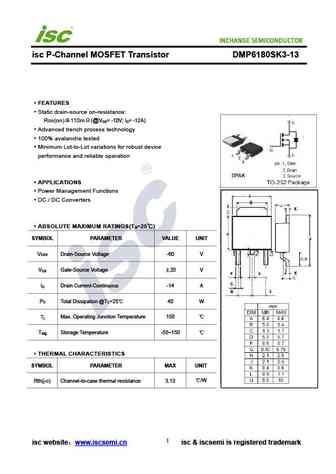
isc P-Channel MOSFET Transistor DMP6180SK3-13 FEATURES Static drain-source on-resistance RDS(on) 110m (@V = -10V; I = -12A) GS D Advanced trench process technology 100% avalanche tested Minimum Lot-to-Lot variations for robust device performance and reliable operation APPLICATIONS Power Management Functions DC / DC Converters ABSOLUTE MAXIMUM RATINGS(T =25 ) ... See More ⇒
dmp6180sk3.pdf
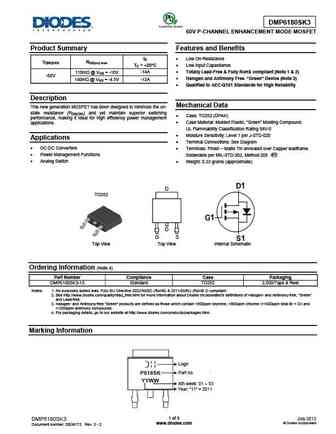
DMP6180SK3 60V P-CHANNEL ENHANCEMENT MODE MOSFET Product Summary Features and Benefits ID Low On-Resistance V(BR)DSS RDS(on) max TC = +25 C Low Input Capacitance Totally Lead-Free & Fully RoHS compliant (Note 1 & 2) 110m @ VGS = -10V -14A -60V Halogen and Antimony Free. Green Device (Note 3) 140m @ VGS = -4.5V -12A Qualified to AEC-Q101 Stand... See More ⇒
dmp6180sk3q.pdf
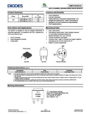
DMP6180SK3Q 60V P-CHANNEL ENHANCEMENT MODE MOSFET Product Summary Features and Benefits ID Low On-Resistance BVDSS RDS(ON) Max TC = +25 C Low Input Capacitance Totally Lead-Free & Fully RoHS Compliant (Note 1 & 2) 110m @ VGS = -10V -14A -60V Halogen and Antimony Free. Green Device (Note 3) 140m @ VGS = -4.5V -12A Qualified to AEC-Q101 Stand... See More ⇒
dmp6180sk3.pdf
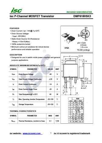
isc P-Channel MOSFET Transistor DMP6180SK3 FEATURES Drain Current I = -14A@ T =25 D C Drain Source Voltage- V = -60V(Min) DSS Static Drain-Source On-Resistance R =110m (Max) DS(on) 100% avalanche tested Minimum Lot-to-Lot variations for robust device performance and reliable operation DESCRIPTION Designed for use in switch mode power supplies and general pu... See More ⇒
Detailed specifications: TSF50N06M, AOT2144L, AOTF12N65L, AOTF2144L, AOTF25S65L, BUZ31H3046, DMG3N60SCT, DMN95H8D5HCT, P60NF06, FCH040N65S3, FCH099N60E, FCH099N65S3, FCP099N60E, FCP125N60E, FCP165N60E, FCP260N65S3, FCP850N80Z
Keywords - DMP6180SK3-13 MOSFET specs
DMP6180SK3-13 cross reference
DMP6180SK3-13 equivalent finder
DMP6180SK3-13 pdf lookup
DMP6180SK3-13 substitution
DMP6180SK3-13 replacement
Learn how to find the right MOSFET substitute. A guide to cross-reference, check specs and replace MOSFETs in your circuits.
History: ELM33415CA
🌐 : EN ES РУ

LIST
Last Update
MOSFET: ASU70R600E | ASU65R850E | ASU65R550E | ASU65R350E | ASR65R120EFD | ASR65R046EFD | ASQ65R046EFD | ASM65R280E | ASM60R330E | ASE70R950E
Popular searches
2sb560 | tip31c transistor equivalent | 2sc1815 datasheet | mj15015 | 13003 transistor datasheet | 2n3416 | bdx53c | k3563