KIA50N06 Specs and Replacement
Type Designator: KIA50N06
Type of Transistor: MOSFET
Type of Control Channel: N-Channel
Absolute Maximum Ratings
Pd ⓘ - Maximum Power Dissipation: 120 W
|Vds|ⓘ - Maximum Drain-Source Voltage: 60 V
|Vgs|ⓘ - Maximum Gate-Source Voltage: 25 V
|Id| ⓘ - Maximum Drain Current: 50 A
Tj ⓘ - Maximum Junction Temperature: 175 °C
Electrical Characteristics
tr ⓘ - Rise Time: 105 nS
Cossⓘ - Output Capacitance: 440 pF
RDSonⓘ - Maximum Drain-Source On-State Resistance: 0.022 Ohm
Package: TO220M-SQ
KIA50N06 substitution
- MOSFET ⓘ Cross-Reference Search
KIA50N06 datasheet
kia50n06.pdf
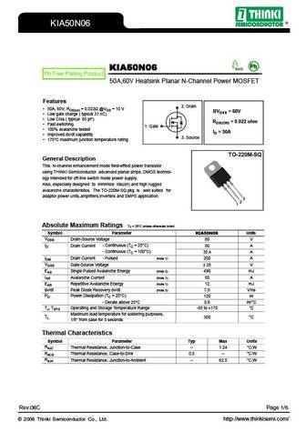
KIA50N06 Pb KIA50N06 Pb Free Plating Product 50A,60V Heatsink Planar N-Channel Power MOSFET Features 2. Drain 50A, 60V, RDS(on) = 0.022 @VGS = 10 V BVDSS = 60V Low gate charge ( typical 31 nC) Low Crss ( typical 65 pF) RDS(ON) = 0.022 ohm Fast switching 1. Gate 100% avalanche tested ID = 50A ... See More ⇒
kia50n06b.pdf
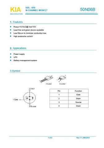
50A 60V 50N06B N-CHANNELMOSFET KIA KIA KIA SEMICONDUCTORS SEMICONDUCTORS SEMICONDUCTORS 1. Features R =10.5m @ V =10V DS(on) GS Lead free and green device available Low Rds-on to minimize conductive loss High avalanche current 2. Applications Power supply UPS Battery management system 3.Symbol Pin Function 1 Gate 2 Drain 3 Source 4 Drain 1of 6 Rev 1.1JAN2014 ... See More ⇒
kia50n03bd.pdf
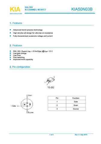
50A30V N-CHANNELMOSFET KIA50N03B KIA KIA KIA SEMICONDUCTORS SEMICONDUCTORS SEMICONDUCTORS 1. Features Advanced trenchprocess technology High density cell design for ultra lowon-resistance Fully characterized avalanche voltage and current 2. Features 50A, 30V, R (on) typ. =6.5m (typ.)@V =10 V DS GS Lowgate charge LowCrss Fast switching Improveddv/dt capability 3. Pinc... See More ⇒
kia50n03.pdf
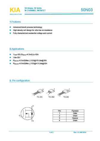
50 Amps, 30 Volts N-CHANNEL MOSFET 50N03 KIA KIA KIA SEMICONDUCTORS SEMICONDUCTORS SEMICONDUCTORS 1.Features Advanced trench process technology High density cell design for ultra low on-resistance Fully characterized avalanche voltage and current 2.Applications VDSS=30V,RDS(on)=6.5m ,ID=50A Vds=30V RDS(ON)=6.5m (Max.),VGS@10V,Ids@30A RDS(... See More ⇒
Detailed specifications: HY1001P, HY3610P, ISA07N65A, JCS13N50FT, JCS3205CH, JCS3205SH, KIA2906A-220, KIA2906A-247, AO3407, NTD4963NG, PFP13N60, PFF13N60, QM3054M6, SVD730D, SVD730F, SVD730T, TP0202T
Keywords - KIA50N06 MOSFET specs
KIA50N06 cross reference
KIA50N06 equivalent finder
KIA50N06 pdf lookup
KIA50N06 substitution
KIA50N06 replacement
Step-by-step guide to finding a MOSFET replacement. Cross-reference parts and ensure compatibility for your repair or project.
History: 2SK1019 | SUD50N04-8M8P | S68N08S | M7002NND03 | RV2C010UN | EMB22A04G | RV1C002UN
🌐 : EN ES РУ

LIST
Last Update
MOSFET: AUB062N08BG | AUB060N08AG | AUB056N10 | AUB056N08BGL | AUB050N085 | AUB050N055 | AUB045N12 | AUB045N10BT | AUB039N10 | AUB034N10
Popular searches
p75nf75 mosfet equivalent | irfpe50 | tip50 | transistor bc547 datasheet | bc109c | d331 transistor | irfbc40 | mp16b transistor