AOTF29S50L Specs and Replacement
Type Designator: AOTF29S50L
Type of Transistor: MOSFET
Type of Control Channel: N-Channel
Absolute Maximum Ratings
Pd ⓘ
- Maximum Power Dissipation: 37.9 W
|Vds|ⓘ - Maximum Drain-Source Voltage: 500 V
|Vgs|ⓘ - Maximum Gate-Source Voltage: 30 V
|Id| ⓘ - Maximum Drain Current: 29 A
Tj ⓘ - Maximum Junction Temperature: 150 °C
Electrical Characteristics
tr ⓘ - Rise Time: 39 nS
Cossⓘ -
Output Capacitance: 88 pF
RDSonⓘ - Maximum Drain-Source On-State Resistance: 0.15 Ohm
Package: TO220F
- MOSFET ⓘ Cross-Reference Search
AOTF29S50L datasheet
..1. Size:441K 1
aot29s50l aob29s50l aotf29s50l aotf29s50.pdf 
AOT29S50L/AOB29S50L/AOTF29S50L/AOTF29S50 TM 500V 29A MOS Power Transistor General Description Product Summary VDS @ Tj,max 600V The AOT29S50L & AOB29S50L & AOTF29S50L & AOTF29S50 have been fabricated using the advanced IDM 120A MOSTM high voltage process that is designed to deliver high RDS(ON),max 0.15 levels of performance and robustness in switching Qg,typ 26.6nC appl... See More ⇒
..2. Size:992K aosemi
aot29s50l aob29s50l aotf29s50l aotf29s50.pdf
AOT29S50L/AOB29S50L/AOTF29S50L/AOTF29S50 TM 500V 29A MOS Power Transistor General Description Product Summary VDS @ Tj,max 600V The AOT29S50L & AOB29S50L & AOTF29S50L & AOTF29S50 have been fabricated using the advanced IDM 120A MOSTM high voltage process that is designed to deliver high RDS(ON),max 0.15 levels of performance and robustness in switching Qg,typ 26.6nC appl... See More ⇒
..3. Size:252K inchange semiconductor
aotf29s50l.pdf

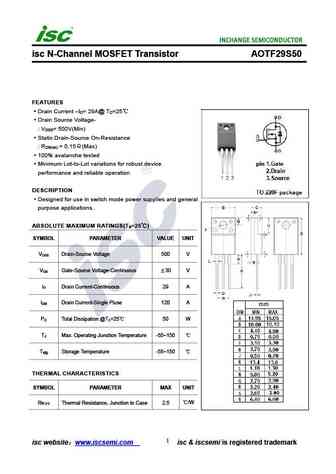
isc N-Channel MOSFET Transistor AOTF29S50L FEATURES Drain Current I = 29A@ T =25 D C Drain Source Voltage- V = 500V(Min) DSS Static Drain-Source On-Resistance R = 0.15 (Max) DS(on) 100% avalanche tested Minimum Lot-to-Lot variations for robust device performance and reliable operation DESCRIPTION Designed for use in switch mode power supplies and general pu... See More ⇒
5.1. Size:324K aosemi
aotf29s50.pdf
AOT29S50/AOB29S50/AOTF29S50 TM 500V 29A MOS Power Transistor General Description Product Summary VDS @ Tj,max 600V The AOT29S50 & AOB29S50 & AOTF29S50 have been fabricated using the advanced MOSTM high voltage IDM 120A process that is designed to deliver high levels of RDS(ON),max 0.15 performance and robustness in switching applications. Qg,typ 26.6nC By provi... See More ⇒
5.2. Size:252K inchange semiconductor
aotf29s50.pdf
isc N-Channel MOSFET Transistor AOTF29S50 FEATURES Drain Current I = 29A@ T =25 D C Drain Source Voltage- V = 500V(Min) DSS Static Drain-Source On-Resistance R = 0.15 (Max) DS(on) 100% avalanche tested Minimum Lot-to-Lot variations for robust device performance and reliable operation DESCRIPTION Designed for use in switch mode power supplies and general pur... See More ⇒
8.1. Size:381K aosemi
aob2910l aot2910l aotf2910l.pdf
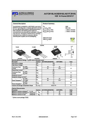
AOT2910L/AOB2910L/AOTF2910L 100V N-Channel MOSFET General Description Product Summary VDS The AOT2910L & AOB2910L & AOTF2910L uses trench 100V MOSFET technology that is uniquely optimized to provide ID (at VGS=10V) 30A / 22A the most efficient high frequency switching performance. RDS(ON) (at VGS=10V) ... See More ⇒
8.2. Size:434K aosemi
aotf2910l.pdf

AOT2910L/AOB2910L/AOTF2910L 100V N-Channel MOSFET General Description Product Summary VDS The AOT2910L & AOB2910L & AOTF2910L uses trench 100V MOSFET technology that is uniquely optimized to provide ID (at VGS=10V) 30A / 22A the most efficient high frequency switching performance. RDS(ON) (at VGS=10V) ... See More ⇒
8.3. Size:378K aosemi
aotf298l.pdf
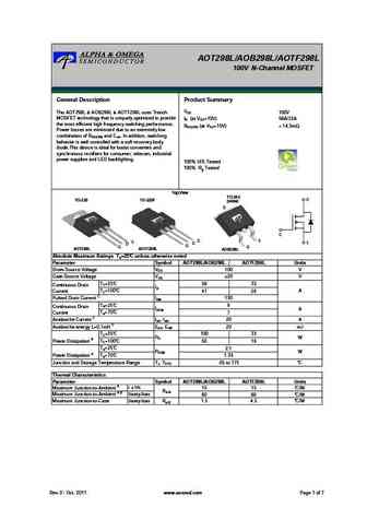
AOT298L/AOB298L/AOTF298L 100V N-Channel MOSFET General Description Product Summary VDS The AOT298L & AOB298L & AOTF298L uses Trench 100V MOSFET technology that is uniquely optimized to provide ID (at VGS=10V) 58A/33A the most efficient high frequency switching performance. RDS(ON) (at VGS=10V) ... See More ⇒
8.4. Size:434K aosemi
aot2910l aob2910l aotf2910l.pdf
AOT2910L/AOB2910L/AOTF2910L 100V N-Channel MOSFET General Description Product Summary VDS The AOT2910L & AOB2910L & AOTF2910L uses trench 100V MOSFET technology that is uniquely optimized to provide ID (at VGS=10V) 30A / 22A the most efficient high frequency switching performance. RDS(ON) (at VGS=10V) ... See More ⇒
8.5. Size:409K aosemi
aotf2916l.pdf
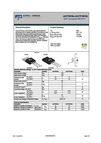
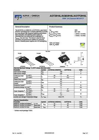
AOT2916L/AOTF2916L 100V N-Channel MOSFET General Description Product Summary VDS The AOT2916L & AOTF2916L uses trench MOSFET 100V technology that is uniquely optimized to provide the most ID (at VGS=10V) 23A / 17A efficient high frequency switching performance. Both RDS(ON) (at VGS=10V) ... See More ⇒
8.6. Size:381K aosemi
aotf2918l.pdf
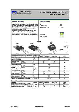
AOT2918L/AOB2918L/AOTF2918L 100V N-Channel MOSFET General Description Product Summary VDS The AOT2918L & AOB2918L & AOTF2918L uses Trench 100V MOSFET technology that is uniquely optimized to provide ID (at VGS=10V) 90A the most efficient high frequency switching performance. RDS(ON) (at VGS=10V) ... See More ⇒
8.7. Size:479K aosemi
aot292l aob292l aotf292l.pdf
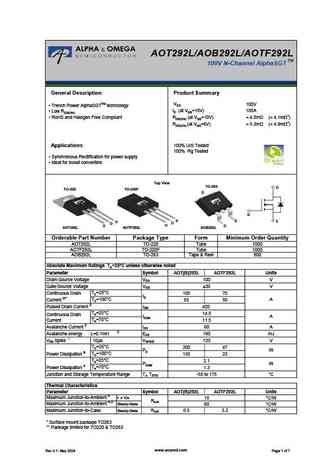
AOT292L/AOB292L/AOTF292L TM 100V N-Channel AlphaSGT General Description Product Summary VDS 100V Trench Power AlphaSGTTM technology ID (at VGS=10V) 105A Low RDS(ON) RoHS and Halogen Free Compliant RDS(ON) (at VGS=10V) ... See More ⇒
8.8. Size:440K aosemi
aotf292l.pdf
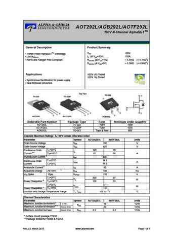
AOT292L/AOB292L/AOTF292L TM 100V N-Channel AlphaSGT General Description Product Summary VDS 100V Trench Power AlphaSGTTM technology ID (at VGS=10V) 105A Low RDS(ON) RoHS and Halogen Free Compliant RDS(ON) (at VGS=10V) ... See More ⇒
8.9. Size:323K aosemi
aotf290l.pdf
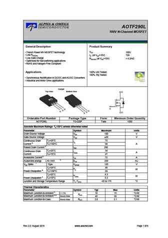
AOTF290L 100V N-Channel MOSFET General Description Product Summary VDS Trench Power MV MOSFET technology 100V Low RDS(ON) ID (at VGS=10V) 72A Low Gate Charge RDS(ON) (at VGS=10V) ... See More ⇒
8.11. Size:581K aosemi
aotf296l.pdf
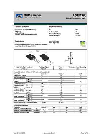
AOTF296L 100V N-Channel MOSFET General Description Product Summary VDS Trench Power MV MOSFET technology 100V Low RDS(ON) ID (at VGS=10V) 41A Low Gate Charge RDS(ON) (at VGS=10V) ... See More ⇒
8.12. Size:236K inchange semiconductor
aotf2910l.pdf

isc N-Channel MOSFET Transistor AOTF2910L FEATURES Drain Current I = 30A@ T =25 D C Drain Source Voltage- V = 100V(Min) DSS Static Drain-Source On-Resistance R = 24m (Max) DS(on) 100% avalanche tested Minimum Lot-to-Lot variations for robust device performance and reliable operation DESCRITION Be suitable for synchronous rectification for server and gen... See More ⇒
8.13. Size:235K inchange semiconductor
aotf298l.pdf
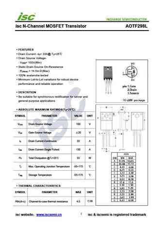
isc N-Channel MOSFET Transistor AOTF298L FEATURES Drain Current I = 33A@ T =25 D C Drain Source Voltage- V = 100V(Min) DSS Static Drain-Source On-Resistance R = 14.5m (Max) DS(on) 100% avalanche tested Minimum Lot-to-Lot variations for robust device performance and reliable operation DESCRITION Be suitable for synchronous rectification for server and ge... See More ⇒
8.14. Size:275K inchange semiconductor
aotf2916l.pdf
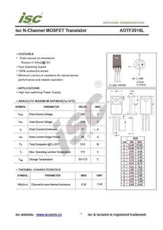
isc N-Channel MOSFET Transistor AOTF2916L FEATURES Drain-source on-resistance RDS(on) 34m @10V Fast Switching Speed 100% avalanche tested Minimum Lot-to-Lot variations for robust device performance and reliable operation APPLICATIONS High fast switching Power Supply ABSOLUTE MAXIMUM RATINGS(T =25 ) a SYMBOL PARAMETER VALUE UNIT V Drain-Source Voltage 100 V... See More ⇒
8.15. Size:236K inchange semiconductor
aotf2918l.pdf

isc N-Channel MOSFET Transistor AOTF2918L FEATURES Drain Current I = 58A@ T =25 D C Drain Source Voltage- V = 100V(Min) DSS Static Drain-Source On-Resistance R = 7m (Max) DS(on) 100% avalanche tested Minimum Lot-to-Lot variations for robust device performance and reliable operation DESCRITION Be suitable for synchronous rectification for server and gene... See More ⇒
8.16. Size:235K inchange semiconductor
aotf292l.pdf

isc N-Channel MOSFET Transistor AOT292L FEATURES Drain Current I = 70A@ T =25 D C Drain Source Voltage- V = 100V(Min) DSS Static Drain-Source On-Resistance R = 4.5m (Max) DS(on) 100% avalanche tested Minimum Lot-to-Lot variations for robust device performance and reliable operation DESCRITION Be suitable for synchronous rectification for server and gene... See More ⇒
8.17. Size:236K inchange semiconductor
aotf290l.pdf

isc N-Channel MOSFET Transistor AOTF290L FEATURES Drain Current I = 72A@ T =25 D C Drain Source Voltage- V = 100V(Min) DSS Static Drain-Source On-Resistance R = 4.2m (Max) DS(on) 100% avalanche tested Minimum Lot-to-Lot variations for robust device performance and reliable operation DESCRITION Be suitable for synchronous rectification for server and gen... See More ⇒
8.18. Size:235K inchange semiconductor
aotf296l.pdf

isc N-Channel MOSFET Transistor AOTF296L FEATURES Drain Current I = 41A@ T =25 D C Drain Source Voltage- V = 100V(Min) DSS Static Drain-Source On-Resistance R = 10m (Max) DS(on) 100% avalanche tested Minimum Lot-to-Lot variations for robust device performance and reliable operation DESCRITION Be suitable for synchronous rectification for server and gene... See More ⇒
Detailed specifications: ME4953, SI4914DY, SSP60N05, SSP60N06, SUV90N06-05, SVF740T, SVF740F, AOB9N70, 10N60, AOTF9N70L, AOW66412, FMV60N190S2HF, JCS650C, JCS650F, JCS650S, R6002END3, R6003KND3
Keywords - AOTF29S50L MOSFET specs
AOTF29S50L cross reference
AOTF29S50L equivalent finder
AOTF29S50L pdf lookup
AOTF29S50L substitution
AOTF29S50L replacement
Step-by-step guide to finding a MOSFET replacement. Cross-reference parts and ensure compatibility for your repair or project.