SSW7N60B Specs and Replacement
Type Designator: SSW7N60B
Type of Transistor: MOSFET
Type of Control Channel: N-Channel
Absolute Maximum Ratings
Pd ⓘ - Maximum Power Dissipation: 147 W
|Vds|ⓘ - Maximum Drain-Source Voltage: 600 V
|Vgs|ⓘ - Maximum Gate-Source Voltage: 30 V
|Id| ⓘ - Maximum Drain Current: 7 A
Tj ⓘ - Maximum Junction Temperature: 150 °C
Electrical Characteristics
tr ⓘ - Rise Time: 80 nS
Cossⓘ - Output Capacitance: 115 pF
RDSonⓘ - Maximum Drain-Source On-State Resistance: 1.2 Ohm
Package: D2PAK
SSW7N60B substitution
- MOSFET ⓘ Cross-Reference Search
SSW7N60B datasheet
ssw7n60b ssi7n60b.pdf
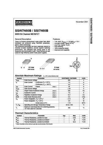
November 2001 SSW7N60B / SSI7N60B 600V N-Channel MOSFET General Description Features These N-Channel enhancement mode power field effect 7.0A, 600V, RDS(on) = 1.2 @VGS = 10 V transistors are produced using Fairchild s proprietary, Low gate charge ( typical 38 nC) planar, DMOS technology. Low Crss ( typical 23 pF) This advanced technology has been especially tailored to ... See More ⇒
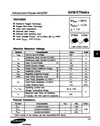
ssw7n60a.pdf
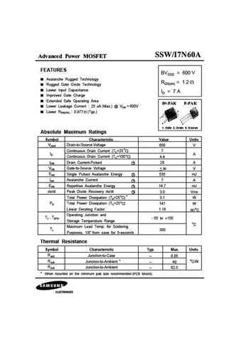
Advanced Power MOSFET FEATURES BVDSS = 600 V Avalanche Rugged Technology RDS(on) = 1.2 Rugged Gate Oxide Technology Lower Input Capacitance ID = 7 A Improved Gate Charge Extended Safe Operating Area Lower Leakage Current 25 A (Max.) @ VDS = 600V 2 Lower RDS(ON) 0.977 (Typ.) 1 1 2 3 3 1. Gate 2. Drain 3. Source Absolute Maximum Ratings Symbol Chara... See More ⇒
Detailed specifications: R6006JNX, R6006KND3, R6006KNX, R6007JND3, R6007JNJ, R6007JNX, SSF7N60B, SSI7N60B, SKD502T, STE40NA60, STE36N50A, STE45NK80ZD, STE38NB50, STE38NB50F, STE24NA100, STE15NA100, AO3409L
Keywords - SSW7N60B MOSFET specs
SSW7N60B cross reference
SSW7N60B equivalent finder
SSW7N60B pdf lookup
SSW7N60B substitution
SSW7N60B replacement
Need a MOSFET replacement? Our guide shows you how to find a perfect substitute by comparing key parameters and specs
History: WMN25N65EM | IRFZ20FI | PMV170UN | SM4805DSK | NCE55P04S | SDM4953A | 2SK4068-01
🌐 : EN ES РУ

LIST
Last Update
MOSFET: AUB034N10 | AUB033N08BG | AUB026N085 | AUA062N08BG | AUA060N08AG | AUA056N08BGL | AUA039N10 | ASW80R290E | ASW65R120EFD | ASW65R110E
Popular searches
c1740 transistor | c828 transistor | c4467 | c2383 transistor | 2n3055 equivalent | s9015 datasheet | 2n6488 | 30j127 datasheet