R6511ENJ Specs and Replacement
Type Designator: R6511ENJ
Type of Transistor: MOSFET
Type of Control Channel: N-Channel
Absolute Maximum Ratings
Pd ⓘ - Maximum Power Dissipation: 124 W
|Vds|ⓘ - Maximum Drain-Source Voltage: 650 V
|Vgs|ⓘ - Maximum Gate-Source Voltage: 20 V
|Id| ⓘ - Maximum Drain Current: 11 A
Tj ⓘ - Maximum Junction Temperature: 150 °C
Electrical Characteristics
tr ⓘ - Rise Time: 35 nS
Cossⓘ - Output Capacitance: 780 pF
RDSonⓘ - Maximum Drain-Source On-State Resistance: 0.4 Ohm
Package: TO-263
R6511ENJ substitution
- MOSFET ⓘ Cross-Reference Search
R6511ENJ datasheet
r6511enj.pdf

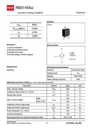
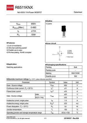
R6511ENJ Datasheet Nch 650V 11A Power MOSFET lOutline l LPT(S) VDSS 650V RDS(on)(Max.) 0.4 ID 11A PD 124W lFeatures l lInner circuit l 1) Low on-resistance 2) Fast switching speed 3) Parallel use is easy 4) Pb-free plating ; RoHS compliant lApplication l lPackaging specifications l Switching Packing Embos... See More ⇒
r6511enj.pdf
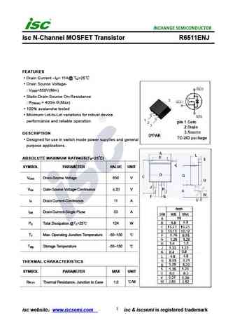
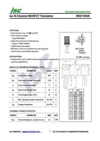
isc N-Channel MOSFET Transistor R6511ENJ FEATURES Drain Current I = 11A@ T =25 D C Drain Source Voltage- V =650V(Min) DSS Static Drain-Source On-Resistance R = 400m (Max) DS(on) 100% avalanche tested Minimum Lot-to-Lot variations for robust device performance and reliable operation DESCRIPTION Designed for use in switch mode power supplies and general purpo... See More ⇒
r6511enx.pdf
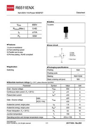
R6511ENX Datasheet Nch 650V 11A Power MOSFET lOutline l TO-220FM VDSS 650V RDS(on)(Max.) 0.4 ID 11A PD 53W lFeatures l lInner circuit l 1) Low on-resistance 2) Fast switching speed 3) Parallel use is easy 4) Pb-free plating ; RoHS compliant lApplication l lPackaging specifications l Switching Packing Bulk... See More ⇒
r6511enx.pdf

isc N-Channel MOSFET Transistor R6511ENX FEATURES Drain Current I = 11A@ T =25 D C Drain Source Voltage- V =650V(Min) DSS Static Drain-Source On-Resistance R = 400m (Max) DS(on) 100% avalanche tested Minimum Lot-to-Lot variations for robust device performance and reliable operation DESCRIPTION Designed for use in switch mode power supplies and general purpo... See More ⇒

Detailed specifications: R6504KNX, R6507ENJ, R6507ENX, R6507KNJ, R6509ENJ, R6509ENX, R6509KNJ, R6509KNX, IRFB4115, R6511ENX, R6511KNJ, R6511KNX, R6515ENJ, R6515ENX, R6515ENZ, R6515KNJ, R6515KNX
Keywords - R6511ENJ MOSFET specs
R6511ENJ cross reference
R6511ENJ equivalent finder
R6511ENJ pdf lookup
R6511ENJ substitution
R6511ENJ replacement
Need a MOSFET replacement? Our guide shows you how to find a perfect substitute by comparing key parameters and specs
🌐 : EN ES РУ

LIST
Last Update
MOSFET: AUB062N08BG | AUB060N08AG | AUB056N10 | AUB056N08BGL | AUB050N085 | AUB050N055 | AUB045N12 | AUB045N10BT | AUB039N10 | AUB034N10
Popular searches
tip36c datasheet | 2sc461 | hy1906 | 2sc2238 | 2sc458 transistor | b649a transistor | 2sa606 | 2n3644