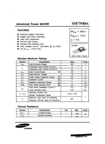
SSF7N80A Specs and Replacement
Type Designator: SSF7N80A
Type of Transistor: MOSFET
Type of Control Channel: N-Channel
Absolute Maximum Ratings
Pd ⓘ
- Maximum Power Dissipation: 90 W
|Vds|ⓘ - Maximum Drain-Source Voltage: 800 V
|Vgs|ⓘ - Maximum Gate-Source Voltage: 30 V
|Id| ⓘ - Maximum Drain Current: 5 A
Tj ⓘ - Maximum Junction Temperature: 150 °C
Electrical Characteristics
tr ⓘ - Rise Time: 40 nS
Cossⓘ -
Output Capacitance: 140 pF
RDSonⓘ - Maximum Drain-Source On-State Resistance: 1.8 Ohm
Package: TO3PF
- MOSFET ⓘ Cross-Reference Search
SSF7N80A datasheet
9.2. Size:660K 1
ssf7n60b.pdf 
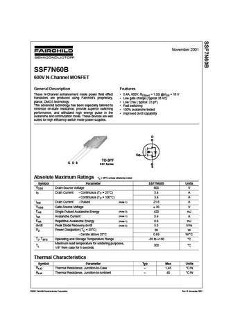
November 2001 SSF7N60B 600V N-Channel MOSFET General Description Features These N-Channel enhancement mode power field effect 5.4A, 600V, RDS(on) = 1.2 @VGS = 10 V transistors are produced using Fairchild s proprietary, Low gate charge ( typical 38 nC) planar, DMOS technology. Low Crss ( typical 23 pF) This advanced technology has been especially tailored to Fast s... See More ⇒
9.3. Size:928K samsung
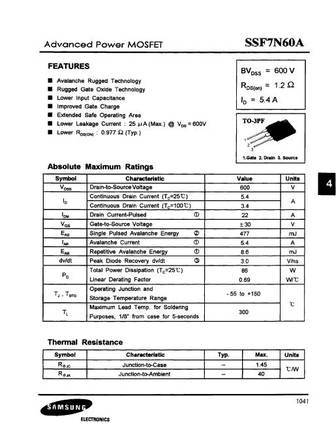
ssf7n90a.pdf
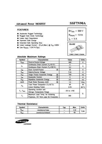
Advanced Power MOSFET FEATURES BVDSS = 900 V Avalanche Rugged Technology RDS(on) = 1.8 Rugged Gate Oxide Technology Lower Input Capacitance ID = 5 A Improved Gate Charge Extended Safe Operating Area Lower Leakage Current 25 A (Max.) @ VDS = 900V Low RDS(ON) 1.247 (Typ.) 1 2 3 1.Gate 2. Drain 3. Source Absolute Maximum Ratings Symbol Characteristic Value Un... See More ⇒
9.4. Size:497K silikron
ssf7ns65g.pdf
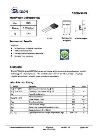
SSF7NS65G Main Product Characteristics VDSS 650V RDS(on) 0.58 (typ.) ID 7A TO-251 Mark in g a nd pin Sch ema tic diag r a m Assignment Features and Benefits Feathers High dv/dt and avalanche capabilities 100% avalanche tested Low input capacitance and gate charge Low gate input resistance Description The SSF7NS65G series MOSFETs is a new t... See More ⇒
9.5. Size:544K silikron
ssf7ns60d.pdf
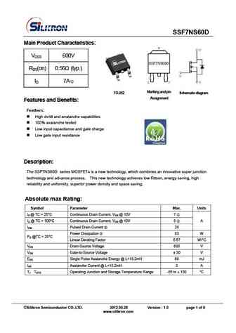
SSF7NS60D Main Product Characteristics VDSS 600V RDS(on) 0.56 (typ.) ID 7A TO-252 Marking a nd p in Sche ma ti c di agr a m Assignment Features and Benefits Feathers High dv/dt and avalanche capabilities 100% avalanche tested Low input capacitance and gate charge Low gate input resistance Description The SSF7NS60D series MOSFETs is a new t... See More ⇒
9.6. Size:433K silikron
ssf7n60.pdf
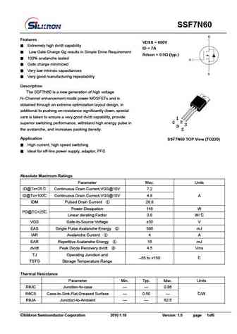
SSF7N60 Features VDSS = 600V Extremely high dv/dt capability ID = 7A Low Gate Charge Qg results in Simple Drive Requirement Rdson = 0.9 (typ.) 100% avalanche tested Gate charge minimized Very low intrinsic capacitances Very good manufacturing repeatability Description The SSF7N60 is a new generation of high voltage N Channel enhancement mode... See More ⇒
9.7. Size:523K silikron
ssf7n60f.pdf
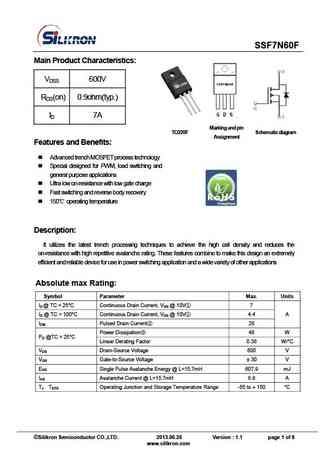
SSF7N60F Main Product Characteristics VDSS 600V RDS(on) 0.9ohm(typ.) ID 7A Marking and p in TO220F Schematic diagram Assignment Features and Benefits Advanced trench MOSFET process technology Special designed for PWM, load switching and general purpose applications Ultra low on-resistance with low gate charge Fast switching and reverse body recovery... See More ⇒
9.8. Size:569K silikron
ssf7ns60f.pdf
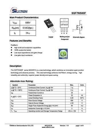
SSF7NS60F Main Product Characteristics VDSS 600V RDS(on) 0.54 (typ.) ID 7A Marking a nd p in Schematic diagram TO220F Assignment Features and Benefits Feathers High dv/dt and avalanche capabilities 100% avalanche tested Low input capacitance and gate charge Low gate input resistance Description The SSF7NS60F series MOSFETs is a new techno... See More ⇒
9.9. Size:462K silikron
ssf7ns70ug.pdf
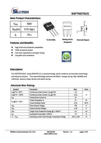
SSF7NS70UG Main Product Characteristics VDSS 700V RDS(on) 0.7 (typ.) ID 7A TO-251 (IPAK) Marking and P in Schematic Diagram Assignment Features and Benefits High dv/dt and avalanche capabilities 100% avalanche tested Low input capacitance and gate charge Low gate input resistance Description The SSF7NS70UG series MOSFETs is a new technology, ... See More ⇒
9.10. Size:449K silikron
ssf7ns65uf.pdf
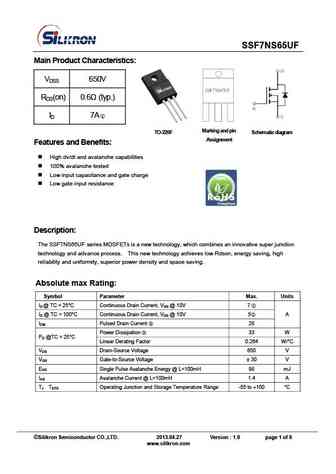
SSF7NS65UF Main Product Characteristics VDSS 650V RDS(on) 0.6 (typ.) ID 7A TO-220F Marking and p in Schematic diagram Assignment Features and Benefits High dv/dt and avalanche capabilities 100% avalanche tested Low input capacitance and gate charge Low gate input resistance Description The SSF7NS65UF series MOSFETs is a new technology, which ... See More ⇒
9.11. Size:485K silikron
ssf7ns65ud.pdf
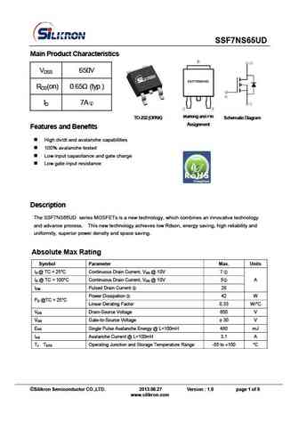
SSF7NS65UD Main Product Characteristics VDSS 650V RDS(on) 0.65 (typ.) ID 7A TO-252 (DPAK) Marking and Pin Schematic Diagram Assignment Features and Benefits High dv/dt and avalanche capabilities 100% avalanche tested Low input capacitance and gate charge Low gate input resistance Description The SSF7NS65UD series MOSFETs is a new technology, whi... See More ⇒
9.12. Size:492K silikron
ssf7n65f.pdf
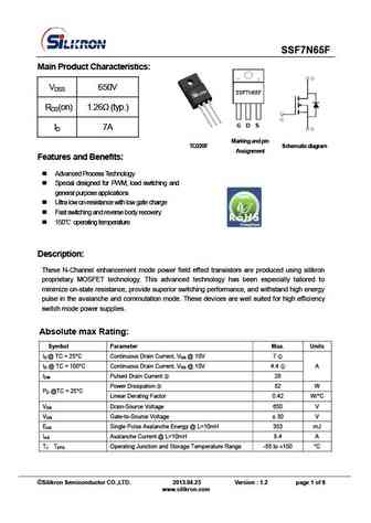
SSF7N65F Main Product Characteristics VDSS 650V RDS(on) 1.26 (typ.) ID 7A Marking and p in TO220F Schematic diagram Assignment Features and Benefits Advanced Process Technology Special designed for PWM, load switching and general purpose applications Ultra low on-resistance with low gate charge Fast switching and reverse body recovery 150 ... See More ⇒
9.13. Size:434K silikron
ssf7ns70ugx.pdf
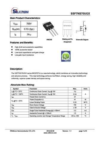
SSF7NS70UGX Main Product Characteristics VDSS 700V RDS(on) 0.7 (typ.) ID 7A IPAK-NX Marking and P in Schematic Diagram Assignment Features and Benefits High dv/dt and avalanche capabilities 100% avalanche tested Low input capacitance and gate charge Low gate input resistance Description The SSF7NS70UGX series MOSFETs is a new technology, whic... See More ⇒
9.14. Size:467K silikron
ssf7ns65ug.pdf

SSF7NS65UG Main Product Characteristics VDSS 650V RDS(on) 0.65 (typ.) ID 7A TO-251 (IPAK) Marking and pin Schematic diagram Assignment Features and Benefits High dv/dt and avalanche capabilities 100% avalanche tested Low input capacitance and gate charge Low gate input resistance Description The SSF7NS65UG series MOSFETs is a new technology, ... See More ⇒
Detailed specifications: SSF4N90AS
, SSF5N80A
, SSF5N90A
, SSF6N70A
, SSF6N80A
, SSF6N90A
, SSF70N10A
, SSF7N60A
, IRFP064N
, SSF7N90A
, SSF80N06A
, SSF8N80A
, SSF8N90A
, SSF9N80A
, SSF9N90A
, SSH10N60A
, SSH10N70
.
Keywords - SSF7N80A MOSFET specs
SSF7N80A cross reference
SSF7N80A equivalent finder
SSF7N80A pdf lookup
SSF7N80A substitution
SSF7N80A replacement
Need a MOSFET replacement?
Our guide shows you how to find a perfect substitute by comparing key parameters and specs