DMP10H4D2S Specs and Replacement
Type Designator: DMP10H4D2S
Type of Transistor: MOSFET
Type of Control Channel: P-Channel
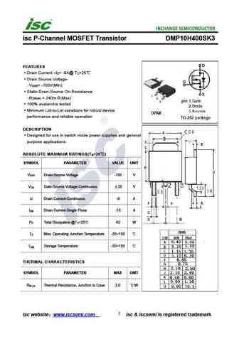
Absolute Maximum Ratings
Pd ⓘ - Maximum Power Dissipation: 0.44 W
|Vds|ⓘ - Maximum Drain-Source Voltage: 100 V
|Vgs|ⓘ - Maximum Gate-Source Voltage: 20 V
|Id| ⓘ - Maximum Drain Current: 0.27 A
Tj ⓘ - Maximum Junction Temperature: 150 °C
Electrical Characteristics
tr ⓘ - Rise Time: 2.6 nS
Cossⓘ - Output Capacitance: 5.6 pF
RDSonⓘ - Maximum Drain-Source On-State Resistance: 4.2 Ohm
Package: SOT23
DMP10H4D2S substitution
- MOSFET ⓘ Cross-Reference Search
DMP10H4D2S datasheet
dmp10h4d2s.pdf
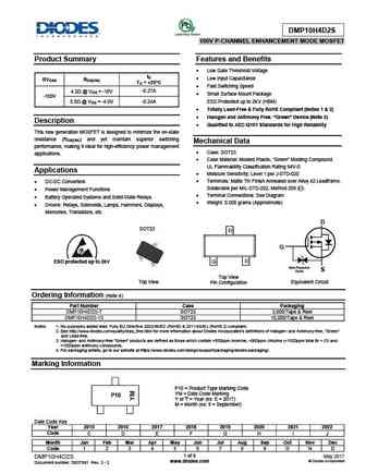
DMP10H4D2S 100V P-CHANNEL ENHANCEMENT MODE MOSFET Product Summary Features and Benefits Low Gate Threshold Voltage ID Low Input Capacitance BVDSS RDS(ON) TA = +25 C Fast Switching Speed 4.2 @ VGS = -10V -0.27A Small Surface Mount Package -100V 5.0 @ VGS = -4.0V -0.24A ESD Protected up to 2KV (HBM) Totally Lead-Free & Fully RoHS Compliant ... See More ⇒
dmp10h400sk3.pdf
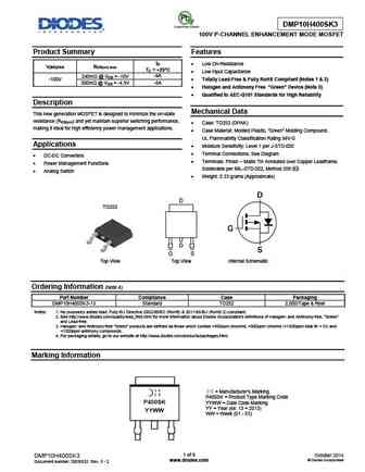
DMP10H400SK3 100V P-CHANNEL ENHANCEMENT MODE MOSFET Product Summary Features ID Low On-Resistance V(BR)DSS RDS(on) max TC = +25 C Low Input Capacitance 240m @ VGS = -10V -9A -100V Totally Lead-Free & Fully RoHS Compliant (Notes 1 & 2) -8A 300m @ VGS = -4.5V Halogen and Antimony Free. Green Device (Note 3) Qualified to AEC-Q101 Standards... See More ⇒
dmp10h400seq.pdf
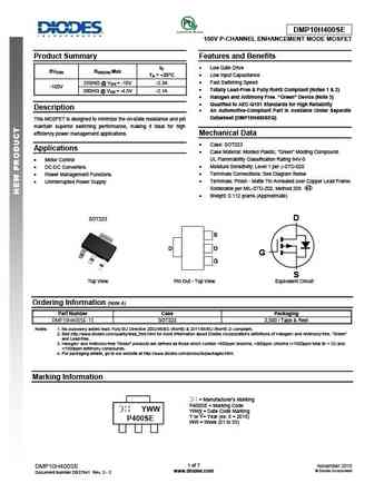
DMP10H400SEQ 100V P-CHANNEL ENHANCEMENT MODE MOSFET Product Summary Features and Benefits ID Low Gate Drive BVDSS RDS(ON) Max TA = +25 C Low Input Capacitance Fast Switching Speed 250m @ VGS = -10V -2.3A -100V Totally Lead-Free & Fully RoHS Compliant (Notes 1 & 2) 300m @ VGS = -4.5V -2.1A Halogen and Antimony Free. Green Device (Note 3) ... See More ⇒
Detailed specifications: DMNH4006SPSQ, DMNH6021SK3Q, DMNH6042SSDQ, DMP1005UFDF, DMP1009UFDF, DMP1055USW, DMP10H400SE, DMP10H400SEQ, EMB04N03H, DMP1100UCB4, DMP2003UPS, DMP2035UFDF, DMP2045U, DMP2088LCP3, DMP2120U, DMP2123LQ, DMP2165UW
Keywords - DMP10H4D2S MOSFET specs
DMP10H4D2S cross reference
DMP10H4D2S equivalent finder
DMP10H4D2S pdf lookup
DMP10H4D2S substitution
DMP10H4D2S replacement
Step-by-step guide to finding a MOSFET replacement. Cross-reference parts and ensure compatibility for your repair or project.
History: 2SK4201-S19-AY | AO3419L
🌐 : EN ES РУ

LIST
Last Update
MOSFET: ASU70R600E | ASU65R850E | ASU65R550E | ASU65R350E | ASR65R120EFD | ASR65R046EFD | ASQ65R046EFD | ASM65R280E | ASM60R330E | ASE70R950E
Popular searches
c2314 transistor | c2482 transistor | 2sc1222 replacement | 2sa725 | c5242 transistor | 2sa726 replacement | a1941 datasheet | hrf3205