3415A Specs and Replacement
Type Designator: 3415A
Type of Transistor: MOSFET
Type of Control Channel: P-Channel
Absolute Maximum Ratings
Pd ⓘ
- Maximum Power Dissipation: 1.4 W
|Vds|ⓘ - Maximum Drain-Source Voltage: 20 V
|Vgs|ⓘ - Maximum Gate-Source Voltage: 10 V
|Id| ⓘ - Maximum Drain Current: 5.6 A
Tj ⓘ - Maximum Junction Temperature: 150 °C
Electrical Characteristics
tr ⓘ - Rise Time: 10 nS
Cossⓘ -
Output Capacitance: 165 pF
RDSonⓘ - Maximum Drain-Source On-State Resistance: 0.04 Ohm
Package: SOT-23
- MOSFET ⓘ Cross-Reference Search
3415A datasheet
..1. Size:2119K goford
3415a.pdf 
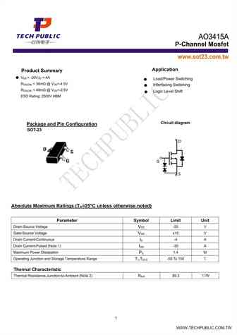
GOFORD 3415A Description The 3415 A uses advanced trench technology to provide excellent RDS(ON), low gate charge and operation with gate voltages as low as1.8V. This device is suitable for use as a load switch or in PWM applications .It is ESD protected. General Features Schematic diagram VDSS RDS(ON) RDS(ON) ID (Typ) @ (Typ) @-2.5V -4.5V 35.8m 46.4m -5.6 -20... See More ⇒
0.1. Size:1291K mcc
si3415a.pdf
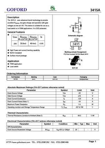
SI3415A Features High Power and Current Handing Capability Epoxy Meets UL 94 V-0 Flammability Rating Moisture Sensitivity Level 1 Halogen Free. Green Device (Note 1) P-Channel Lead Free Finish/RoHS Compliant ("P" Suffix Designates RoHS Compliant. See Ordering Information) MOSFET Maximum Ratings Operating Junction Temperature Range -55oC to +150oC ... See More ⇒
0.2. Size:319K aosemi
ao3415a.pdf
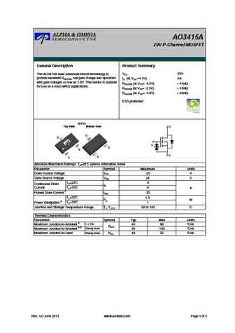
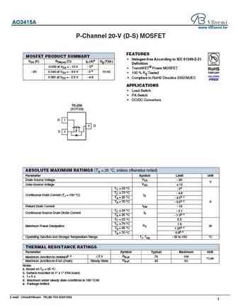
AO3415A 20V P-Channel MOSFET General Description Product Summary VDS -20V The AO3415A uses advanced trench technology to provide excellent RDS(ON), low gate charge and operation ID (at VGS=-4.5V) -5A with gate voltages as low as 1.8V. This device is suitable RDS(ON) (at VGS= -4.5V) ... See More ⇒
0.3. Size:292K cystek
btc3415a3.pdf
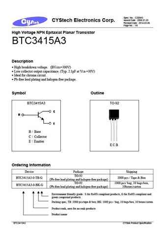
Spec. No. C209A3 Issued Date 2008.01.25 CYStech Electronics Corp. Revised Date 2014.03.06 Page No. 1/6 High Voltage NPN Epitaxial Planar Transistor BTC3415A3 Description High breakdown voltage. (BV =300V) CEO Low collector output capacitance. (Typ. 2.1pF at V =30V) CB Ideal for chroma circuit. Pb-free lead plating and halogen-free package. Symbo... See More ⇒
0.4. Size:1729K kexin
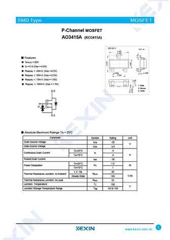
ao3415a.pdf
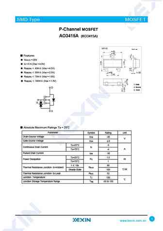
SMD Type MOSFET P-Channel MOSFET AO3415A (KO3415A) SOT-23 Unit mm +0.1 2.9-0.1 +0.1 0.4 -0.1 Features 3 VDS (V) =-20V ID =-5 A (VGS =-4.5V) RDS(ON) 43m (VGS =-4.5V) 1 2 +0.1 0.95-0.1 0.1+0.05 RDS(ON) 55m (VGS =-2.5V) -0.01 +0.1 1.9-0.1 RDS(ON) 75m (VGS =-1.8V) RDS(ON) 100m (VGS =-1.5V) 1. Gate 2. Source D 3. Dra... See More ⇒
0.5. Size:385K kexin
ko3415a.pdf
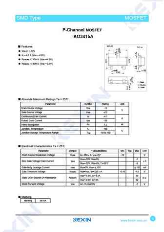
SMD Type MOSFET Transistors P-Channel MOSFET KO3415A SOT-23 Features Unit mm +0.1 2.9 -0.1 +0.1 VDS (V) =-12V 0.4-0.1 3 ID =-4.1 A (VGS =-4.5V) RDS(ON) 45m (VGS =-4.5V) RDS(ON) 60m (VGS =-2.5V) 1 2 +0.1 +0.05 0.95 -0.1 0.1 -0.01 +0.1 1.9 -0.1 1. Gate 2. Source 3. Drain Absolute Maximum Ratings Ta = 25 Parameter Symbol Rating U... See More ⇒
0.6. Size:1662K kexin
ao3415as.pdf
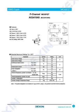
SMD Type MOSFET P-Channel MOSFET AO3415AS (KO3415AS) SOT-23-3 Unit mm +0.2 2.9 -0.1 +0.1 0.4-0.1 Features 3 VDS (V) =-20V ID =-4A (VGS =-4.5V) RDS(ON) 45m (VGS =-4.5V) 1 2 +0.02 +0.1 0.15 -0.02 0.95 -0.1 D RDS(ON) 54m (VGS =-2.5V) +0.1 1.9 -0.2 RDS(ON) 75m (VGS =-1.8V) ESD Rating 3000V HBM G 1. Gate 2. Source 3. Dra... See More ⇒
0.7. Size:1694K kexin
ao3415a-3.pdf
SMD Type MOSFET P-Channel MOSFET AO3415A (KO3415A) SOT-23-3 Unit mm +0.2 2.9 -0.1 +0.1 0.4 -0.1 3 Features VDS (V) =-20V ID =-5 A (VGS =-4.5V) 1 2 RDS(ON) 43m (VGS =-4.5V) +0.02 +0.1 0.15 -0.02 0.95 -0.1 +0.1 1.9 -0.2 RDS(ON) 55m (VGS =-2.5V) RDS(ON) 75m (VGS =-1.8V) RDS(ON) 100m (VGS =-1.5V) 1. Gate 2. Source ... See More ⇒
0.8. Size:394K panjit
pja3415ae.pdf
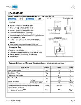
PPJA3415AE 20V P-Channel Enhancement Mode MOSFET ESD Protected SOT-23 Unit inch(mm) Voltage -20 V Current -4.3A Features RDS(ON) , VGS@-4.5V, ID@-4.3A... See More ⇒
0.9. Size:814K ait semi
am3415a.pdf
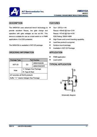
AM3415A AiT Semiconductor Inc. www.ait-ic.com MOSFET P-CHANNEL ENHANCEMENT MODE POWER MOSFET DESCRIPTION FEATURES The AM3415A uses advanced trench technology to V = -20V,I =-4A DS D provide excellent R , low gate charge and R ... See More ⇒
0.10. Size:357K semtron
smc3415a.pdf
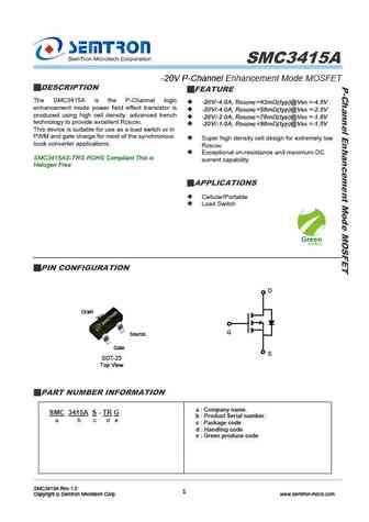
SMC3415A -20V P-Channel Enhancement Mode MOSFET DESCRIPTION FEATURE The SMC3415A is the P-Channel logic -20V/-4.0A, RDS(ON) =43m (typ)@VGS =-4.5V enhancement mode power field effect transistor is -20V/-4.0A, RDS(ON) =58m (typ)@VGS =-2.5V produced using high cell density. advanced trench -20V/-2.0A, RDS(ON) =78m (typ)@VGS =-1.8V technology to provide excel... See More ⇒
0.11. Size:459K umw-ic
ao3415a.pdf
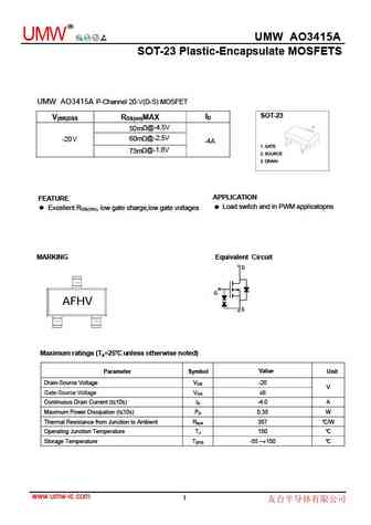
R UMW UMW AO3415A SOT-23 Plastic-Encapsulate MOSFETS UMW AO3415A P-Channel 20-V(D-S) MOSFET SOT-23 ID V(BR)DSS RDS(on)MAX 50m @-4.5V -20V 60m @-2.5V -4A 1. GATE 73m @-1.8V 2. SOURCE 3. DRAIN APPLICATION FEATURE Load switch and in PWM applicatopns Excellent RDS(ON), low gate charge,low gate voltages MARKING Equivalent Circuit D G AFHV S Maximum ratings... See More ⇒
0.12. Size:801K hx
hx3415a.pdf
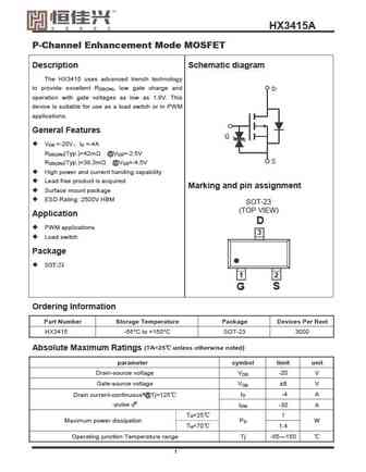
HX3415A P-Channel Enhancement Mode MOSFET Description Schematic diagram The HX3415 uses advanced trench technology to provide excellent R , low gate charge and DS(ON) operation with gate voltages as low as 1.8V. This device is suitable for use as a load switch or in PWM applications. General Features V =-20V I =-4A DS D R (Typ.)=42m @V =-2.5V DS(ON) GS R (Typ.)=38.3m @... See More ⇒
0.13. Size:298K msksemi
ao3415ai-ms.pdf
www.msksemi.com AO3415AI-MS Semiconductor Compiance D VDS -20V I (at V =-4.5V) -4A D GS R (at V = -4.5V) ... See More ⇒
0.14. Size:1604K winsok
wst3415a.pdf
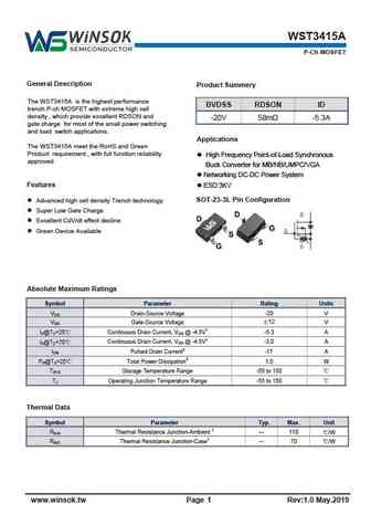
WST3415A P-Ch MOSFET General Description Product Summery The WST3415A is the highest performance BVDSS RDSON ID trench P-ch MOSFET with extreme high cell density , which provide excellent RDSON and -20V 58m -5.3A gate charge for most of the small power switching and load switch applications. Applications The WST3415A meet the RoHS and Green Product requirement , with fu... See More ⇒
0.17. Size:1058K cn yangzhou yangjie elec
yjq3415a.pdf
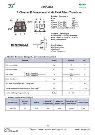
RoHS COMPLIANT YJQ3415A P-Channel Enhancement Mode Field Effect Transistor Product Summary V -20V DS I -6.2A D R ( at V =-4.5V) 42 mohm DS(ON) GS R ( at V =-2.5V) 55 mohm DS(ON) GS R ( at V =-1.8V) 100 mohm DS(ON) GS ESD Protected Up to 4.0KV (HBM) General Description Trench Power LV MOSFET technology High Density Cell Des... See More ⇒
0.18. Size:560K cn yangzhou yangjie elec
yjl3415a.pdf
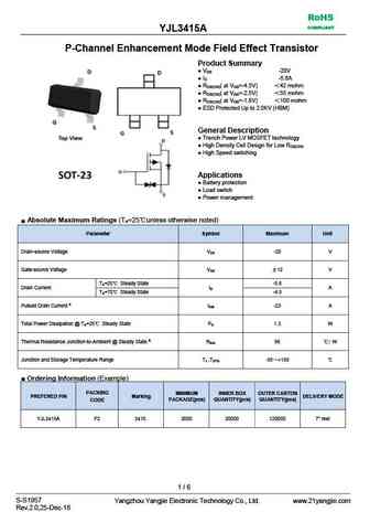
RoHS COMPLIANT YJL3415A P-Channel Enhancement Mode Field Effect Transistor Product Summary V -20V DS I -5.6A D R ( at V =-4.5V) 42 mohm DS(ON) GS R ( at V =-2.5V) 55 mohm DS(ON) GS R ( at V =-1.8V) 100 mohm DS(ON) GS ESD Protected Up to 2.0KV (HBM) General Description Trench Power LV MOSFET technology High Density Cell Des... See More ⇒
0.19. Size:1148K cn apm
ap3415a.pdf
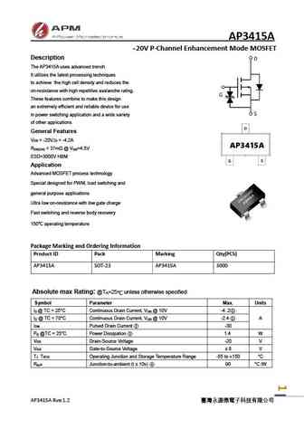
AP3415A -20V P-Channel Enhancement Mode MOSFET Description The AP3415A uses advanced trench It utilizes the latest processing techniques to achieve the high cell density and reduces the on-resistance with high repetitive avalanche rating. These features combine to make this design an extremely efficient and reliable device for use in power switching application and a wide var... See More ⇒
Detailed specifications: BRFL7N80, BRFL8N60, IRFB3710, 2312, 06N06L, 18N10W, 2300F, 3400H, 12N60, 80N06-251, 8680A, G01N20R, G06N10, G08N03D2, G08N06S, G1006LE, G1007
Keywords - 3415A MOSFET specs
3415A cross reference
3415A equivalent finder
3415A pdf lookup
3415A substitution
3415A replacement
Need a MOSFET replacement?
Our guide shows you how to find a perfect substitute by comparing key parameters and specs