G110N06K Specs and Replacement
Type Designator: G110N06K
Type of Transistor: MOSFET
Type of Control Channel: N-Channel
Absolute Maximum Ratings
Pd ⓘ - Maximum Power Dissipation: 120 W
|Vds|ⓘ - Maximum Drain-Source Voltage: 55 V
|Vgs|ⓘ - Maximum Gate-Source Voltage: 20 V
|Id| ⓘ - Maximum Drain Current: 110 A
Tj ⓘ - Maximum Junction Temperature: 175 °C
Electrical Characteristics
tr ⓘ - Rise Time: 15 nS
Cossⓘ - Output Capacitance: 380 pF
RDSonⓘ - Maximum Drain-Source On-State Resistance: 0.0064 Ohm
Package: TO-252
G110N06K substitution
- MOSFET ⓘ Cross-Reference Search
G110N06K datasheet
g110n06k.pdf
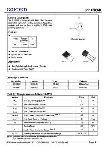
GOFORD G110N06K General Description The G110N06 is N-channel MOS Field Effect Transistor designed for high current switching applications. Rugged EAS capability and ultra low R is suitable for PWM, load DS(ON) switching applications. Features VDSS RDS(ON) ID Schematic diagram @ 10V (Typ) 55V 5.2 m 110A Ultra Low On-Resistance High UIS and UIS 100% Tes... See More ⇒
g110n06 to252 to251.pdf
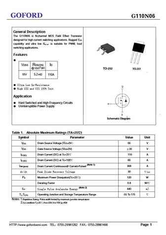
GOFORD G110N06 General Description The G110N06 is N-channel MOS Field Effect Transistor designed for high current switching applications. Rugged EAS capability and ultra low R is suitable for PWM, load DS(ON) switching applications. Features VDSS RDS(ON) ID @ 10V (Typ) TO-252 TO-251 55V 5.2 m 110A Ultra Low On-Resistance High UIS and UIS 100% Test... See More ⇒
g110n06 to220.pdf
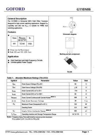
GOFORD G110N06 General Description The G110N06 is N-channel MOS Field Effect Transistor designed for high current switching applications. Rugged EAS capability and ultra low R is suitable for PWM, load DS(ON) switching applications. Features Schematic diagram VDSS RDS(ON) ID @ 10V (Typ) 55V 5.2 m 110A Ultra Low On-Resistance High UIS and UIS 100% Te... See More ⇒
g110n06 to252.pdf
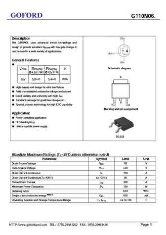
GOFORD G110N06. Description The G110N06. uses advanced trench technology and design to provide excellent R with low gate charge. It DS(ON) can be used in a wide variety of applications. General Features Schematic diagram VDSS RDS(ON) RDS(ON) ID @ 4.5V (Typ) @ 10V (Typ) m m 110 55V 5.8 5.4 A High density cell design for ultra low Rdson Fully characteriz... See More ⇒
Detailed specifications: 8680A, G01N20R, G06N10, G08N03D2, G08N06S, G1006LE, G1007, G10N10A, IRFP450, G12P10K, G13N04, G15N10C, G16P03, G16P03S, G18N20K, G1NP02ELL, G2003A
Keywords - G110N06K MOSFET specs
G110N06K cross reference
G110N06K equivalent finder
G110N06K pdf lookup
G110N06K substitution
G110N06K replacement
Step-by-step guide to finding a MOSFET replacement. Cross-reference parts and ensure compatibility for your repair or project.
History: HM120N03K | BRD70N08 | G06N10 | BRF5N65 | IXCY01N90E
🌐 : EN ES РУ

LIST
Last Update
MOSFET: AUB034N10 | AUB033N08BG | AUB026N085 | AUA062N08BG | AUA060N08AG | AUA056N08BGL | AUA039N10 | ASW80R290E | ASW65R120EFD | ASW65R110E
Popular searches
2n4249 datasheet | tip130 | se9302 transistor | fr5305 datasheet | y2 transistor | 40n06 | bc108b | oc84