SSP6N70A Specs and Replacement
Type Designator: SSP6N70A
Type of Transistor: MOSFET
Type of Control Channel: N-Channel
Absolute Maximum Ratings
Pd ⓘ - Maximum Power Dissipation: 130 W
|Vds|ⓘ - Maximum Drain-Source Voltage: 700 V
|Vgs|ⓘ - Maximum Gate-Source Voltage: 30 V
|Id| ⓘ - Maximum Drain Current: 6 A
Tj ⓘ - Maximum Junction Temperature: 150 °C
Electrical Characteristics
tr ⓘ - Rise Time: 23 nS
Cossⓘ - Output Capacitance: 100 pF
RDSonⓘ - Maximum Drain-Source On-State Resistance: 1.8 Ohm
Package: TO220
SSP6N70A substitution
- MOSFET ⓘ Cross-Reference Search
SSP6N70A datasheet
ssp6n70a.pdf

Advanced Power MOSFET FEATURES BVDSS = 700 V Avalanche Rugged Technology RDS(on) = 1.8 Rugged Gate Oxide Technology Lower Input Capacitance ID = 6 A Improved Gate Charge Extended Safe Operating Area Lower Leakage Current 25 A (Max.) @ VDS = 700V Low RDS(ON) 1.552 (Typ.) 1 2 3 1.Gate 2. Drain 3. Source Absolute Maximum Ratings Symbol Characteristic Value ... See More ⇒
ssp6n80a.pdf
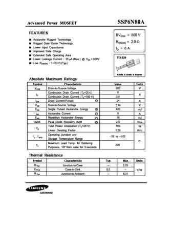
Advanced Power MOSFET FEATURES BVDSS = 800 V Avalanche Rugged Technology RDS(on) = 2.0 Rugged Gate Oxide Technology Lower Input Capacitance ID = 6 A Improved Gate Charge Extended Safe Operating Area Lower Leakage Current 25 A (Max.) @ VDS = 800V Low RDS(ON) 1. (Typ.) 1 2 3 1.Gate 2. Drain 3. Source 1.Gate 2. Drain 3. Source Absolute Maximum Ratings Symb... See More ⇒
ssp6n90a.pdf
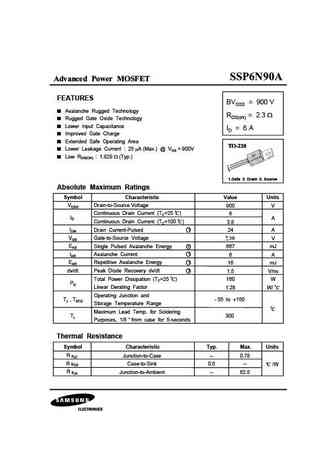
Advanced Power MOSFET FEATURES BVDSS = 900 V Avalanche Rugged Technology RDS(on) = 2.3 Rugged Gate Oxide Technology Lower Input Capacitance ID = 6 A Improved Gate Charge Extended Safe Operating Area Lower Leakage Current 25 A (Max.) @ VDS = 900V Low RDS(ON) 1.829 (Typ.) 1 2 3 1.Gate 2. Drain 3. Source Absolute Maximum Ratings Symbol Characteristic Value ... See More ⇒
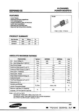
Detailed specifications: SSP4N80A , SSP4N80AS , SSP4N90A , SSP4N90AS , SSP5N80A , SSP5N90A , SSP6N55 , SSP6N60 , IRFP064N , SSP6N80A , SSP6N90A , SSP70N10A , SSP7N60A , SSP7N80A , SSP80N06A , SSR1N50 , SSR1N50A .
Keywords - SSP6N70A MOSFET specs
SSP6N70A cross reference
SSP6N70A equivalent finder
SSP6N70A pdf lookup
SSP6N70A substitution
SSP6N70A replacement
Need a MOSFET replacement? Our guide shows you how to find a perfect substitute by comparing key parameters and specs
