HY1503C1 Datasheet. Specs and Replacement
Type Designator: HY1503C1
Type of Transistor: MOSFET
Type of Control Channel: N-Channel
Absolute Maximum Ratings
Pd ⓘ - Maximum Power Dissipation: 17.8 W
|Vds|ⓘ - Maximum Drain-Source Voltage: 30 V
|Vgs|ⓘ - Maximum Gate-Source Voltage: 20 V
|Id| ⓘ - Maximum Drain Current: 34 A
Tj ⓘ - Maximum Junction Temperature: 150 °C
Electrical Characteristics
tr ⓘ - Rise Time: 12.5 nS
Cossⓘ - Output Capacitance: 150 pF
RDSonⓘ - Maximum Drain-Source On-State Resistance: 0.0085 Ohm
Package: DFN3X3-8L
HY1503C1 substitution
- MOSFET ⓘ Cross-Reference Search
HY1503C1 datasheet
hy1503c1.pdf
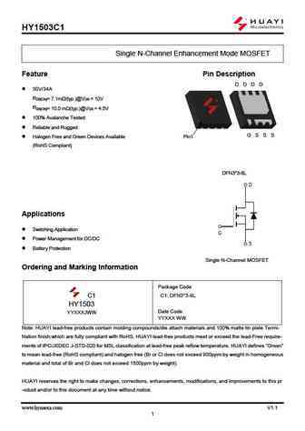
HY1503C1 Single N-Channel Enhancement Mode MOSFET Feature Pin Description D D D D 30V/34A RDS(ON)= 7.1m (typ.)@VGS = 10V RDS(ON)= 10.0 m (typ.)@VGS = 4.5V 100% Avalanche Tested Reliable and Rugged G S S S Halogen Free and Green Devices Available Pin1 (RoHS Compliant) DFN3*3-8L Applications Switching Application Power Management for DC/D... See More ⇒
hy1506c2.pdf
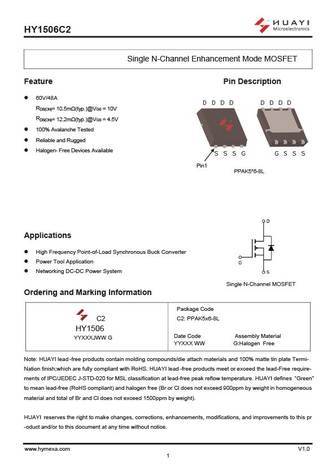
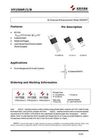
HY1506C2 Single N-Channel Enhancement Mode MOSFET Feature Pin Description 60V/48A D D D D D D D D RDS(ON)= 10.5m (typ.)@VGS = 10V RDS(ON)= 12.2m (typ.)@VGS = 4.5V 100% Avalanche Tested Reliable and Rugged Halogen- Free Devices Available S S S G G S S S Pin1 PPAK5*6-8L Applications High Frequency Point-of-Load Synchronous Buck Converter Power Tool Application ... See More ⇒
hy150n075t.pdf
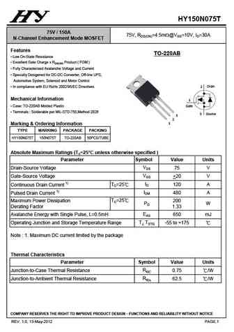
SINGLE FIG.SINGLE PHASE HALF WAVE 60Hz DERATING CURVE FIG. 2 MAXIMUM NON- T1 FORWARD CURRENT AMBIENT TEMPERATURE ( ) 1 2 5 10 1 25 50 75 10 20 150 175 0.00 0.2 0.4 0.6 4 100 125 100 HY150N075T 75V / 150A 75V, RDS(ON)=4.5mW@VGS=10V, ID=30A N-Channel Enhancement Mode MOSFET Features TO-220AB Low On-State Resistance Excellent Gate Charge x RDS(ON) Product ... See More ⇒
hy1506c2.pdf
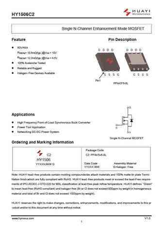
HY1506C2 Single N-Channel Enhancement Mode MOSFET Feature Pin Description 60V/48A D D D D D D D D RDS(ON)= 10.5m (typ.)@VGS = 10V RDS(ON)= 12.2m (typ.)@VGS = 4.5V 100% Avalanche Tested Reliable and Rugged Halogen- Free Devices Available S S S G G S S S Pin1 PPAK5*6-8L Applications High Frequency Point-of-Load Synchronous Buck Converter Power Tool Application ... See More ⇒
Detailed specifications: HY12P03S, HY1303C, HY1310D, HY1310U, HY1310V, HY1403D, HY1403U, HY1403V, IRF540, HY1506C2, HY15P03C2, HY15P03S, HY1603D, HY1603U, HY1603S, HY1603P, HY1603B
Keywords - HY1503C1 MOSFET specs
HY1503C1 cross reference
HY1503C1 equivalent finder
HY1503C1 pdf lookup
HY1503C1 substitution
HY1503C1 replacement
Can't find your MOSFET? Learn how to find a substitute transistor by analyzing voltage, current and package compatibility
🌐 : EN ES РУ

LIST
Last Update
MOSFET: ASDM40N60KQ | ASDM40N40E | ASDM40N100P | ASDM40DN20E | ASDM3416EZA | ASDM3415ZA | ASDM3401ZA | ASDM3401 | ASDM3400ZA | ASDM30P30BE
Popular searches
2sc1775 | 2n1305 | 2sc5242 | irf540 equivalent | mp1620 transistor equivalent | 2sc945 transistor | c2073 transistor | ac176 transistor