HY1607U Datasheet. Specs and Replacement
Type Designator: HY1607U
Type of Transistor: MOSFET
Type of Control Channel: N-Channel
Absolute Maximum Ratings
Pd ⓘ - Maximum Power Dissipation: 75 W
|Vds|ⓘ - Maximum Drain-Source Voltage: 68 V
|Vgs|ⓘ - Maximum Gate-Source Voltage: 25 V
|Id| ⓘ - Maximum Drain Current: 70 A
Tj ⓘ - Maximum Junction Temperature: 175 °C
Electrical Characteristics
tr ⓘ - Rise Time: 13 nS
Cossⓘ - Output Capacitance: 351 pF
RDSonⓘ - Maximum Drain-Source On-State Resistance: 0.0085 Ohm
Package: TO251
HY1607U substitution
- MOSFET ⓘ Cross-Reference Search
HY1607U datasheet
hy1607d hy1607u hy1607v.pdf
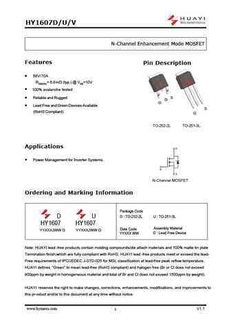
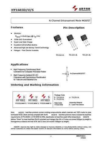
HY1607D/U/V N-Channel Enhancement Mode MOSFET Features Pin Description 68V/70A RDS(ON)= 6.8m (typ.) @ VGS=10V 100% avalanche tested Reliable and Rugged S D G Lead Free and Green Devices Available S D (RoHS Compliant) G TO-252-2L TO-251-3L Applications Power Management for Inverter Systems. N-Channel MOSFET Ordering and Marking Information Package Cod... See More ⇒
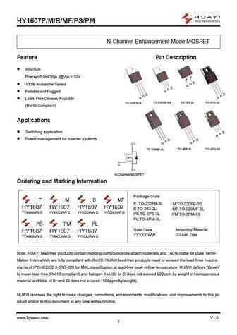
hy1607p hy1607m hy1607b hy1607mf hy1607ps hy1607pm.pdf
S D G S D G S S D D G G TO-220FB-3L TO-220FB-3M TO-263-2L TO-3PM-3L S D G S S D ... See More ⇒
hy1607p.pdf
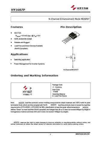
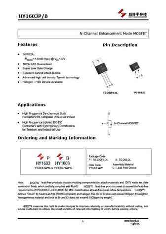
HY1607P N-Channel Enhancement Mode MOSFET Features Pin Description 68V/70A RDS(ON)= 6.5m (typ.) @ VGS=10V 100% avalanche tested G D Reliable and Rugged S Lead Free and Green Devices Available D (RoHS Compliant) Applications G Switching application Power Management for Inverter Systems. S N-Channel MOSFET Ordering and Marking Information Package Code P T... See More ⇒
hy1606p hy1606b.pdf

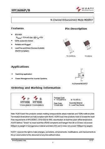
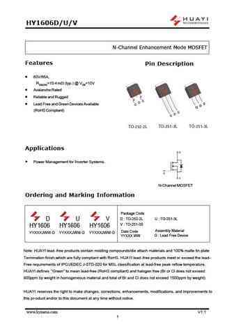
HY1606P/B N-Channel Enhancement Mode MOSFET Features Pin Description 60V/66A RDS(ON)= 10.4 m (typ.) @ VGS=10V 100% avalanche tested Reliable and Rugged S Lead Free and Green Devices Available D G (RoHS Compliant) S D G TO-220FB-3L TO-263-2L Applications Switching application Power Management for Inverter Systems. N-Channel MOSFET Ordering and ... See More ⇒
Detailed specifications: HY1603U, HY1603S, HY1603P, HY1603B, HY1606D, HY1606U, HY1606V, HY1607D, 10N60, HY1607V, HY1607M, HY1607B, HY1607MF, HY1607PS, HY1607PM, HY1710P, HY1710M
Keywords - HY1607U MOSFET specs
HY1607U cross reference
HY1607U equivalent finder
HY1607U pdf lookup
HY1607U substitution
HY1607U replacement
Step-by-step guide to finding a MOSFET replacement. Cross-reference parts and ensure compatibility for your repair or project.
🌐 : EN ES РУ

LIST
Last Update
MOSFET: RM50P30DF | CRTT095N12N | CRSS028N10N | CRST030N10N | CRJQ80N65F | ASDM20N20KQ | ASDM20N100Q | ASDM12N65F | ASDM100R750PKQ | ASDM100R160NKQ
Popular searches
tta004b | 2sc1116 | 2n3565 equivalent | 10n60 | 2sc1061 | a1023 | d313 transistor | 2sa1302