SSS4N55 Datasheet. Specs and Replacement
Type Designator: SSS4N55 📄📄
Type of Transistor: MOSFET
Type of Control Channel: N-Channel
Absolute Maximum Ratings
Pd ⓘ - Maximum Power Dissipation: 35 W
|Vds|ⓘ - Maximum Drain-Source Voltage: 550 V
|Id| ⓘ - Maximum Drain Current: 4 A
Tj ⓘ - Maximum Junction Temperature: 150 °C
Electrical Characteristics
RDSonⓘ - Maximum Drain-Source On-State Resistance: 3 Ohm
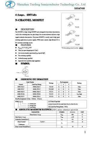
Package: TO220F
📄📄 Copy
SSS4N55 substitution
- MOSFET ⓘ Cross-Reference Search
SSS4N55 datasheet
ssp4n60b sss4n60b.pdf
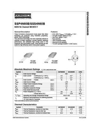
SSP4N60B/SSS4N60B 600V N-Channel MOSFET General Description Features These N-Channel enhancement mode power field effect 4.0A, 600V, RDS(on) = 2.5 @VGS = 10 V transistors are produced using Fairchild s proprietary, Low gate charge ( typical 22 nC) planar, DMOS technology. Low Crss ( typical 14 pF) This advanced technology has been especially tailored to Fast switchi... See More ⇒
sss4n80as.pdf
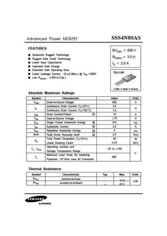
SSS4N80AS Advanced Power MOSFET FEATURES BVDSS = 800 V Avalanche Rugged Technology RDS(on) = 3.0 Rugged Gate Oxide Technology Lower Input Capacitance ID = 2.8 A Improved Gate Charge Extended Safe Operating Area TO-220F Lower Leakage Current 25 A (Max.) @ VDS = 800V Low RDS(ON) 2.450 (Typ.) 1 2 3 1.Gate 2. Drain 3. Source Absolute Maximum Ratings Symbol C... See More ⇒
sss4n80a.pdf

Advanced Power MOSFET FEATURES BVDSS = 800 V Avalanche Rugged Technology RDS(on) = 4.0 Rugged Gate Oxide Technology Lower Input Capacitance ID = 2.5 A Improved Gate Charge Extended Safe Operating Area Lower Leakage Current 25 A (Max.) @ VDS = 800V Low RDS(ON) 3.400 (Typ.) 1 2 3 1.Gate 2. Drain 3. Source Absolute Maximum Ratings Symbol Characteristic Valu... See More ⇒
sss4n90a.pdf

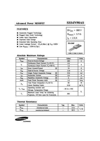
Advanced Power MOSFET FEATURES BVDSS = 900 V Avalanche Rugged Technology RDS(on) = 5.0 Rugged Gate Oxide Technology Lower Input Capacitance ID = 2.5 A Improved Gate Charge Extended Safe Operating Area Lower Leakage Current 25 A (Max.) @ VDS = 900V Low RDS(ON) 4.181 (Typ.) 1 2 3 1.Gate 2. Drain 3. Source Absolute Maximum Ratings Symbol Characteristic Valu... See More ⇒

Detailed specifications: SSS10N60A, SSS1N50A, SSS1N60A, SSS2N60A, SSS2N80A, SSS2N90A, SSS3N80A, SSS3N90A, 8205A, SSS4N60, SSS4N60AS, SSS4N80A, SSS4N80AS, SSS4N90A, SSS4N90AS, SSS5N80A, SSS5N90A
Keywords - SSS4N55 MOSFET specs
SSS4N55 cross reference
SSS4N55 equivalent finder
SSS4N55 pdf lookup
SSS4N55 substitution
SSS4N55 replacement
Can't find your MOSFET? Learn how to find a substitute transistor by analyzing voltage, current and package compatibility
MOSFET Parameters. How They Affect Each Other
🌐 : EN ES РУ

LIST
Last Update
MOSFET: CS95118 | CS85105A | CS75N45 | CS72N12 | CS55N50 | CS48N75A | CS40N27 | MSQ60P04D | MSQ40P07D | MSQ30P40D
Popular searches
2sc1815 datasheet | mj15015 | 13003 transistor datasheet | 2n3416 | bdx53c | k3563 | d882p | 2sb1560