SSW7N60A Specs and Replacement
Type Designator: SSW7N60A
Type of Transistor: MOSFET
Type of Control Channel: N-Channel
Absolute Maximum Ratings
Pd ⓘ - Maximum Power Dissipation: 147 W
|Vds|ⓘ - Maximum Drain-Source Voltage: 600 V
|Vgs|ⓘ - Maximum Gate-Source Voltage: 30 V
|Id| ⓘ - Maximum Drain Current: 7 A
Tj ⓘ - Maximum Junction Temperature: 150 °C
Electrical Characteristics
tr ⓘ - Rise Time: 19 nS
Cossⓘ - Output Capacitance: 130 pF
RDSonⓘ - Maximum Drain-Source On-State Resistance: 1.2 Ohm
Package: TO263
SSW7N60A substitution
- MOSFET ⓘ Cross-Reference Search
SSW7N60A datasheet
ssw7n60a.pdf
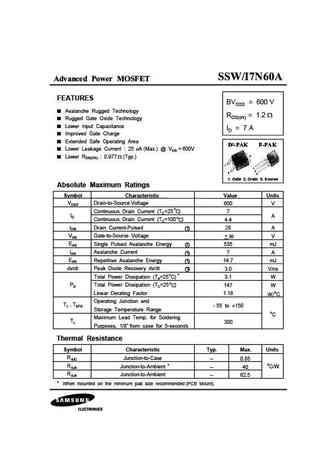
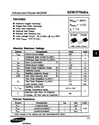
Advanced Power MOSFET FEATURES BVDSS = 600 V Avalanche Rugged Technology RDS(on) = 1.2 Rugged Gate Oxide Technology Lower Input Capacitance ID = 7 A Improved Gate Charge Extended Safe Operating Area Lower Leakage Current 25 A (Max.) @ VDS = 600V 2 Lower RDS(ON) 0.977 (Typ.) 1 1 2 3 3 1. Gate 2. Drain 3. Source Absolute Maximum Ratings Symbol Chara... See More ⇒
ssw7n60b ssi7n60b.pdf
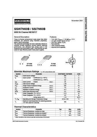
November 2001 SSW7N60B / SSI7N60B 600V N-Channel MOSFET General Description Features These N-Channel enhancement mode power field effect 7.0A, 600V, RDS(on) = 1.2 @VGS = 10 V transistors are produced using Fairchild s proprietary, Low gate charge ( typical 38 nC) planar, DMOS technology. Low Crss ( typical 23 pF) This advanced technology has been especially tailored to ... See More ⇒
Detailed specifications: SSW4N60A , SSW4N80A , SSW4N80AS , SSW4N90A , SSW4N90AS , SSW5N80A , SSW5N90A , SSW6N70A , AO4407 , STD10N10-1 , STD10N10L-1 , STD10N10LT4 , STD10N10T4 , STD12N05 , STD12N05-1 , STD12N05L , STD12N05L-1 .
History: PMV48XP
Keywords - SSW7N60A MOSFET specs
SSW7N60A cross reference
SSW7N60A equivalent finder
SSW7N60A pdf lookup
SSW7N60A substitution
SSW7N60A replacement
Need a MOSFET replacement? Our guide shows you how to find a perfect substitute by comparing key parameters and specs
History: PMV48XP
🌐 : EN ES РУ

LIST
Last Update
MOSFET: HAF1008S | HAF1008L | EMZB08P03H | CS30N20FA9R | AOT66613L | AOSP21313C | AOSP21311C | AOB66918L | AO3415C | AOTF20N40L
Popular searches
2sc5198 | 2sc1971 | tip41c transistor datasheet | 2n3907 | 12n60 | mp42b transistor | c1675 transistor | c5198 transistor