IPB08CN10NG Datasheet. Specs and Replacement
Type Designator: IPB08CN10NG 📄📄
Type of Transistor: MOSFET
Type of Control Channel: N-Channel
Absolute Maximum Ratings
Pd ⓘ - Maximum Power Dissipation: 167 W
|Vds|ⓘ - Maximum Drain-Source Voltage: 100 V
|Vgs|ⓘ - Maximum Gate-Source Voltage: 20 V
|Id| ⓘ - Maximum Drain Current: 95 A
Tj ⓘ - Maximum Junction Temperature: 175 °C
Electrical Characteristics
tr ⓘ - Rise Time: 24 nS
Cossⓘ - Output Capacitance: 757 pF
RDSonⓘ - Maximum Drain-Source On-State Resistance: 0.0082 Ohm
Package: TO263
📄📄 Copy
- MOSFET ⓘ Cross-Reference Search
IPB08CN10NG datasheet
..1. Size:527K infineon
ipb08cn10ng ipi08cn10ng ipp08cn10ng.pdf 
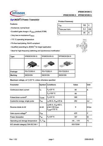
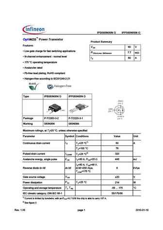
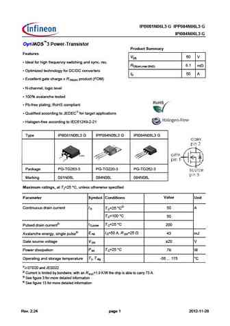
IPB08CN10N G IPI08CN10N G IPP08CN10N G OptiMOS 2 Power-Transistor Product Summary Features V 100 V DS N-channel, normal level R 8.2 m DS(on),max (TO263) Excellent gate charge x R product (FOM) DS(on) I 95 A D Very low on-resistance R DS(on) 175 C operating temperature Pb-free lead plating; RoHS compliant Qualified according to JEDEC1) for target ... See More ⇒
7.1. Size:772K infineon
ipi08cne8n-g ipp08cne8n-g ipb08cne8n-g ipp08cne8n7.pdf
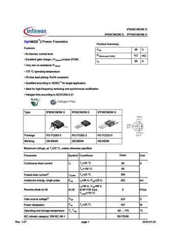
IPB08CNE8N G IPI08CNE8N G IPP08CNE8N G 2 Power-Transistor Product Summary Features V D R ( 492??6= ?@C>2= =6G6= R m - @? >2I .) R I46==6?E 82E6 492C86 I R AC@5F4E !) ' D n) I D R /6CJ =@H @? C6D DE2?46 R D n) R U @A6C2E ?8 E6>A6C2EFC6 R *3 7C66 =625 A=2E ?8 , @#- 4@>A= 2?E 1) R + F2= 7 65 244@C5 ?8 E@ % 7@C E2C86E 2AA= 42E @? R $562= 7@C 9 89 7C6BF6?4J DH E49 ?8... See More ⇒
9.1. Size:778K infineon
ipp086n10n3g ipi086n10n3g ipb083n10n3g ipd082n10n3g.pdf

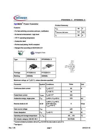
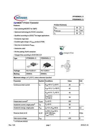
IPP086N10N3 G IPI086N10N3 G IPB083N10N3 G IPD082N10N3 G OptiMOS 3 Power-Transistor Product Summary Features VDS 100 V N-channel, normal level RDS(on),max (TO 252) 8.2 mW Excellent gate charge x R product (FOM) DS(on) ID 80 A Very low on-resistance R DS(on) 175 C operating temperature Pb-free lead plating; RoHS compliant Qualified according to JED... See More ⇒
9.2. Size:737K infineon
ipb085n06lg.pdf
IPB085N06L G IPP085N06L G Power-Transistor Product Summary Features V D P ?A 61BC BF9C389>7 3?>E5AC5AB 1>4 BH>3 A53C96931C9?> R m , ?> =1G ,' E5AB9?> P ( 381>>581>35=5>C ... See More ⇒
9.3. Size:739K infineon
ipb085n06lg ipp085n06lg.pdf

IPB085N06L G IPP085N06L G Power-Transistor Product Summary Features V D P ?A 61BC BF9C389>7 3?>E5AC5AB 1>4 BH>3 A53C96931C9?> R m , ?> =1G ,' E5AB9?> P ( 381>>581>35=5>C ... See More ⇒
9.4. Size:683K infineon
ipb081n06l3g ipp084n06l3g ipb081n06l3 ipp084n06l3 ipb084n06l33.pdf
pe IPB081N06L3 G IPP084N06L3 G 3 Power-Transistor Product Summary Features V D R #562= 7@C 9 89 7C6BF6?4J DH E49 ?8 2?5 DJ?4 C64 R 1 m - @? >2I -' R ) AE > K65 E649?@=@8J 7@C 4@?G6CE6CD I D R I46==6?E 82E6 492C86 I R AC@5F4E ) ' D n) R ( 492??6= =@8 4 =6G6= R 2G2=2?496 E6DE65 R *3 7C66 A=2E ?8 , @"- 4@>A= 2?E 1) R + F2= 7 65 244@C5 ?8 E@ $ 7@C E2C86E 2AA= 42E @?... See More ⇒
9.5. Size:908K infineon
ipb083n15n5lf.pdf
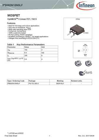
IPB083N15N5LF MOSFET D PAK OptiMOSTM 5 Linear FET, 150 V Features Ideal for hot-swap and e-fuse applications Very low on-resistance R DS(on) Wide safe operating area SOA N-channel, normal level 100% avalanche tested Pb-free plating; RoHS compliant Qualified according to JEDEC1) for target applications Halogen-free according to IEC61249-2-21 Drain ... See More ⇒
9.6. Size:739K infineon
ipb080n06ng ipp080n06ng.pdf
IPB080N06N G IPP080N06N G Power-Transistor Product Summary Features V D P &?F 71C5 381A75 6?A 61BC BF9C389>7 1@@B R 7 7 m , ?> =1G ,' E5AB9?> P ( 381>>581>35=5>C >?A=1... See More ⇒
9.7. Size:726K infineon
ipb080n03l.pdf
Type IPP080N03L G IPB080N03L G 3 Power-Transistor Product Summary Features V 30 V DS Fast switching MOSFET for SMPS R 8.0 mW DS(on),max Optimized technology for DC/DC converters I 50 A D Qualified according to JEDEC1) for target applications N-channel, logic level Excellent gate charge x R product (FOM) DS(on) Very low on-resistance R DS(on) ... See More ⇒
9.8. Size:757K infineon
ipp086n10n3-g ipi086n10n3-g ipb083n10n3-g ipd082n10n3-g.pdf
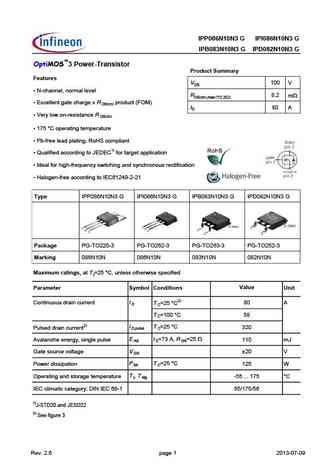
IPP086N10N3 G IPI086N10N3 G IPB083N10N3 G IPD082N10N3 G OptiMOS 3 Power-Transistor Product Summary Features VDS 100 V N-channel, normal level RDS(on),max (TO 252) 8.2 mW Excellent gate charge x R product (FOM) DS(on) ID 80 A Very low on-resistance R DS(on) 175 C operating temperature Pb-free lead plating; RoHS compliant Qualified according to JED... See More ⇒
9.9. Size:427K infineon
ipb081n06l3g ipp084n06l3g ipi084n06l3g ipi084n06l3g.pdf
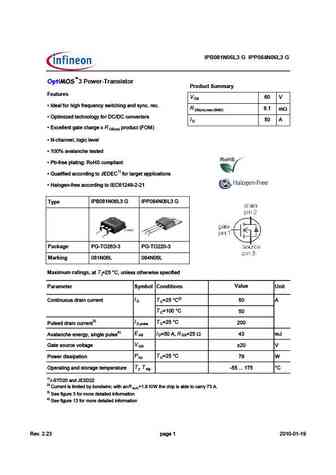
Type IPB081N06L3 G IPP084N06L3 G IPI084N06L3 G OptiMOS 3 Power-Transistor Product Summary Features VDS 60 V Ideal for high frequency switching and sync. rec. RDS(on),max (SMD) 8.1 m Optimized technology for DC/DC converters ID 50 A Excellent gate charge x R product (FOM) DS(on) N-channel, logic level 100% avalanche tested Pb-free plating; RoHS complian... See More ⇒
9.10. Size:258K inchange semiconductor
ipb083n15n5lf.pdf
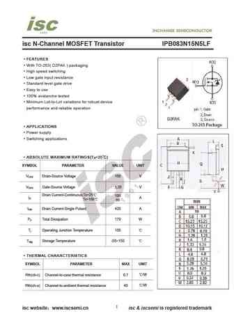
isc N-Channel MOSFET Transistor IPB083N15N5LF FEATURES With TO-263( D2PAK ) packaging High speed switching Low gate input resistance Standard level gate drive Easy to use 100% avalanche tested Minimum Lot-to-Lot variations for robust device performance and reliable operation APPLICATIONS Power supply Switching applications ABSOLUTE MAXIMUM RATINGS(T =25 ) ... See More ⇒
9.11. Size:243K inchange semiconductor
ipb080n03l.pdf
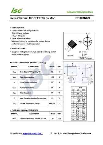
isc N-Channel MOSFET Transistor IPB080N03L DESCRIPTION Drain Current I = 50A@ T =25 D C Drain Source Voltage V = 30V(Min) DSS 100% avalanche tested Minimum Lot-to-Lot variations for robust device performance and reliable operation APPLICATIONS . Designed for high current, high speed switching, switch mode power supplies. ABSOLUTE MAXIMUM RATINGS(T =25 ) C SY... See More ⇒
9.12. Size:258K inchange semiconductor
ipb081n06l3.pdf

Isc N-Channel MOSFET Transistor IPB081N06L3 FEATURES With To-263(D2PAK) package Low input capacitance and gate charge Low gate input resistance 100% avalanche tested Minimum Lot-to-Lot variations for robust device performance and reliable operation APPLICATIONS Switching applications ABSOLUTE MAXIMUM RATINGS(T =25 ) a SYMBOL PARAMETER VALUE UNIT V Drain-Source V... See More ⇒
9.13. Size:258K inchange semiconductor
ipb083n10n3.pdf
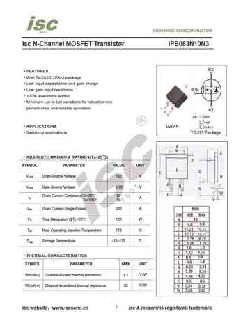
Isc N-Channel MOSFET Transistor IPB083N10N3 FEATURES With To-263(D2PAK) package Low input capacitance and gate charge Low gate input resistance 100% avalanche tested Minimum Lot-to-Lot variations for robust device performance and reliable operation APPLICATIONS Switching applications ABSOLUTE MAXIMUM RATINGS(T =25 ) a SYMBOL PARAMETER VALUE UNIT V Drain-Source V... See More ⇒
Detailed specifications: IGOT60R070D1, IGT60R070D1, IGT60R190D1S, IPA60R180P7S, IPA60R360P7S, IPAN60R180P7S, IPAN65R650CE, IPB015N04N6, IRF3205, IPB100N12S3-05, IPB120N10S4-03, IPB120N10S4-05, IPB120P04P4L-03, IPB180N04S4L-01, IPB180N04S4L-H0, IPB180N08S4-02, IPB180N10S4-02
Keywords - IPB08CN10NG MOSFET specs
IPB08CN10NG cross reference
IPB08CN10NG equivalent finder
IPB08CN10NG pdf lookup
IPB08CN10NG substitution
IPB08CN10NG replacement
Need a MOSFET replacement?
Our guide shows you how to find a perfect substitute by comparing key parameters and specs
