IPD25DP06NM Specs and Replacement
Type Designator: IPD25DP06NM
Type of Transistor: MOSFET
Type of Control Channel: P-Channel
Absolute Maximum Ratings
Pd ⓘ - Maximum Power Dissipation: 28 W
|Vds|ⓘ - Maximum Drain-Source Voltage: 60 V
|Vgs|ⓘ - Maximum Gate-Source Voltage: 20 V
|Id| ⓘ - Maximum Drain Current: 6.5 A
Tj ⓘ - Maximum Junction Temperature: 175 °C
Electrical Characteristics
tr ⓘ - Rise Time: 7 nS
Cossⓘ - Output Capacitance: 62 pF
RDSonⓘ - Maximum Drain-Source On-State Resistance: 0.25 Ohm
Package: TO252
IPD25DP06NM substitution
- MOSFET ⓘ Cross-Reference Search
IPD25DP06NM datasheet
ipd25dp06nm.pdf
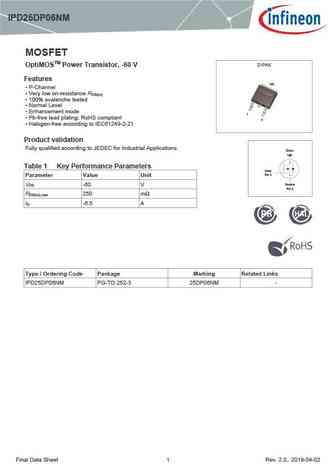
IPD25DP06NM MOSFET D-PAK OptiMOSTM Power Transistor, -60 V Features tab P-Channel Very low on-resistance R DS(on) 100% avalanche tested Normal Level Enhancement mode 1 Pb-free lead plating; RoHS compliant 3 Halogen-free according to IEC61249-2-21 Product validation Fully qualified according to JEDEC for Industrial Applications Drain tab Table 1 Ke... See More ⇒
ipd25dp06lm.pdf
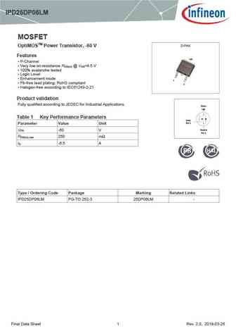
IPD25DP06LM MOSFET D-PAK OptiMOSTM Power Transistor, -60 V Features tab P-Channel Very low on-resistance R @ V =4.5 V DS(on) GS 100% avalanche tested Logic Level Enhancement mode 1 Pb-free lead plating; RoHS compliant 3 Halogen-free according to IEC61249-2-21 Product validation Fully qualified according to JEDEC for Industrial Applications Drain ta... See More ⇒
ipd250n06n3.pdf
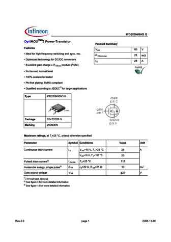
pe # ! ! # A03 B53 R m D n) m x Q ( @D9=9J54 D538>?F5BD5BC I D Q H35>5?B=1... See More ⇒
ipb26cn10ng ipd25cn10ng ipi26cn10ng ipp26cn10ng.pdf
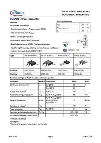
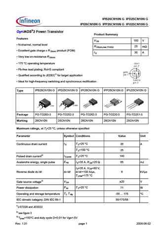
IPB26CN10N G IPD25CN10N G IPI26CN10N G IPP26CN10N G OptiMOS 2 Power-Transistor Product Summary Features VDS 100 V N-channel, normal level RDS(on),max (TO252) 25 mW Excellent gate charge x R product (FOM) DS(on) ID 35 A Very low on-resistance R DS(on) 175 C operating temperature Pb-free lead plating; RoHS compliant Qualified according to JEDEC1) ... See More ⇒
Detailed specifications: IPC50N04S5L-5R5, IPC70N04S5-4R6, IPC70N04S5L-4R2, IPC90N04S5-3R6, IPC90N04S5L-3R3, IPD090N03LGE8177, IPD100N04S4L-02, IPD25DP06LM, AON6380, IPD30N12S3L-31, IPD35N12S3L-24, IPD380P06NM, IPD40DP06NM, IPD50N08S4-13, IPD50N12S3L-15, IPD50P04P4-13, IPD60N10S4-12
Keywords - IPD25DP06NM MOSFET specs
IPD25DP06NM cross reference
IPD25DP06NM equivalent finder
IPD25DP06NM pdf lookup
IPD25DP06NM substitution
IPD25DP06NM replacement
Need a MOSFET replacement? Our guide shows you how to find a perfect substitute by comparing key parameters and specs
🌐 : EN ES РУ

LIST
Last Update
MOSFET: AUP060N055 | AUP056N10 | AUP056N08BGL | AUP052N085 | AUP045N12 | AUP039N10 | AUP034N10 | AUP034N06 | AUP033N08BG | AUP026N085
Popular searches
s9018 | 2n3904 equivalent | ksa1220 | s9015 | mje3055t datasheet | a733 | irf9630 | mj2955