ME2328 Specs and Replacement
Type Designator: ME2328
Type of Transistor: MOSFET
Type of Control Channel: N-Channel
Absolute Maximum Ratings
Pd ⓘ - Maximum Power Dissipation: 1.3 W
|Vds|ⓘ - Maximum Drain-Source Voltage: 105 V
|Vgs|ⓘ - Maximum Gate-Source Voltage: 20 V
|Id| ⓘ - Maximum Drain Current: 1.5 A
Tj ⓘ - Maximum Junction Temperature: 150 °C
Electrical Characteristics
tr ⓘ - Rise Time: 6 nS
Cossⓘ - Output Capacitance: 38 pF
RDSonⓘ - Maximum Drain-Source On-State Resistance: 0.27 Ohm
Package: SOT-23
ME2328 substitution
- MOSFET ⓘ Cross-Reference Search
ME2328 datasheet
me2328 me2328-g.pdf
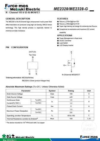
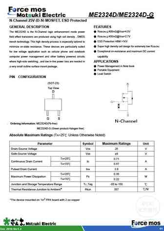
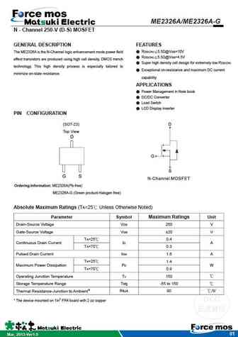
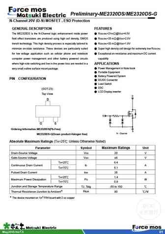
ME2328/ME2328-G N - Channel 105-V (D-S) MOSFET GENERAL DESCRIPTION FEATURES RDS(ON) 270m @VGS=10V The ME2328 is the N-Channel logic enhancement mode power field RDS(ON) 340m @VGS=4.5V effect transistors are produced using high cell density, DMOS trench Super high density cell design for extremely low RDS(ON) technology. This high density process is especiall... See More ⇒
me2323d me2323d-g.pdf
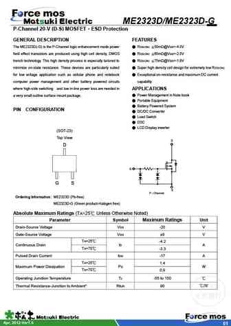
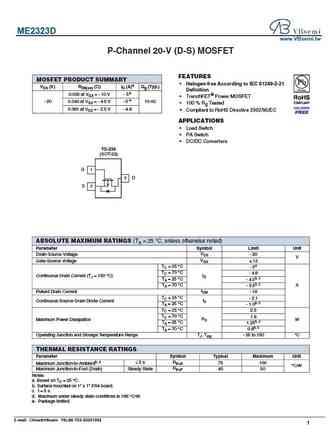
ME2323D/ME2323D-G P-Channel 20-V (D-S) MOSFET ESD Protection GENERAL DESCRIPTION FEATURES The ME2323D(-G) is the P-Channel logic enhancement mode power RDS(ON) 50m @VGS=-4.5V field effect transistors are produced using high cell density, DMOS RDS(ON) 65m @VGS=-2.5V trench technology. This high density process is especially tailored to RDS(ON) 75m @VGS=-1.8... See More ⇒
me2320d me2320d-g.pdf
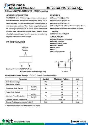
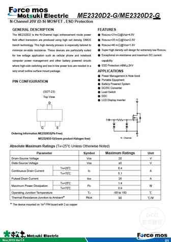
ME2320D/ME2320D-G N-Channel 20V (D-S) MOSFET , ESD Protection GENERAL DESCRIPTION FEATURES The ME2320D is the N-Channel logic enhancement mode power RDS(ON)=21m @VGS=4.5V field effect transistors are produced using high cell density, DMOS RDS(ON)=25 m @VGS=2.5V trench technology. This high density process is especially tailored to RDS(ON)=40 m @VGS=1.8V minimize on-st... See More ⇒
me2325s me2325s-g.pdf
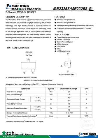
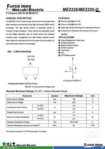
ME2325S/ME2325S-G P-Channel 30V (D-S) MOSFET GENERAL DESCRIPTION FEATURES RDS(ON) 50m @VGS=-10V The ME2325S is the P-Channel logic enhancement mode power field RDS(ON) 76m @VGS=-4.5V effect transistors are produced using high cell density, DMOS trench Super high density cell design for extremely low RDS(ON) technology. This high density process is especially ... See More ⇒
Detailed specifications: ME2320D, ME2320D-G, ME2323D, ME2323D-G, ME2325, ME2325-G, ME2326A, ME2326A-G, 5N60, ME2328-G, ME2333, ME2333-G, ME2345A, ME2345A-G, ME25N06, ME25N06-G, ME2602
Keywords - ME2328 MOSFET specs
ME2328 cross reference
ME2328 equivalent finder
ME2328 pdf lookup
ME2328 substitution
ME2328 replacement
Learn how to find the right MOSFET substitute. A guide to cross-reference, check specs and replace MOSFETs in your circuits.
History: FKV575
🌐 : EN ES РУ

LIST
Last Update
MOSFET: AUB034N10 | AUB033N08BG | AUB026N085 | AUA062N08BG | AUA060N08AG | AUA056N08BGL | AUA039N10 | ASW80R290E | ASW65R120EFD | ASW65R110E
Popular searches
2sc1175 | 2sc632 | mje15030 transistor equivalent | 13003b | 2n6121 | 2sc1312 | bf495 transistor equivalent | 2sc1313