2SK3019A Specs and Replacement
Type Designator: 2SK3019A
Type of Transistor: MOSFET
Type of Control Channel: N-Channel
Absolute Maximum Ratings
Pd ⓘ
- Maximum Power Dissipation: 0.15 W
|Vds|ⓘ - Maximum Drain-Source Voltage: 30 V
|Vgs|ⓘ - Maximum Gate-Source Voltage: 20 V
|Id| ⓘ - Maximum Drain Current: 0.1 A
Tj ⓘ - Maximum Junction Temperature: 150 °C
Electrical Characteristics
tr ⓘ - Rise Time: 35 nS
Cossⓘ -
Output Capacitance: 9 pF
RDSonⓘ - Maximum Drain-Source On-State Resistance: 8 Ohm
Package: SOT523
- MOSFET ⓘ Cross-Reference Search
2SK3019A datasheet
..1. Size:1125K mcc
2sk3019a.pdf 
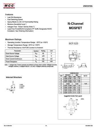
2SK3019A Features Low ON-Resistance Fast Switching Speed Epoxy Meets UL 94 V-0 Flammability Rating Moisture Sensitivity Level 1 N-Channel Halogen Free. Green Device (Note 1) MOSFET Lead Free Finish/RoHS Compliant ("P" Suffix Designates RoHS Compliant. See Ordering Information) Maximum Ratings Operating Junction Temperature Range -55 C to +150 C... See More ⇒
7.1. Size:70K rohm
2sk3019.pdf
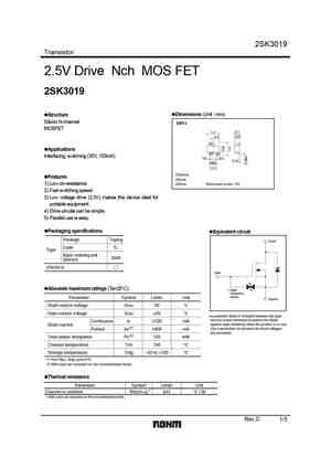
2SK3019 Transistor 2.5V Drive Nch MOS FET 2SK3019 Dimensions (Unit mm) Structure Silicon N-channel EMT3 MOSFET 1.6 0.7 0.55 0.3 ( ) 3 Applications ( ) ( ) 2 1 Interfacing, switching (30V, 100mA) 0.2 0.2 0.15 0.5 0.5 1.0 (1)Source Features (2)Gate 1) Low on-resistance. (3)Drain Abbreviated symbol KN 2) Fast switching speed. 3) Low voltage drive (2.5... See More ⇒
7.2. Size:953K rohm
2sk3019eb.pdf
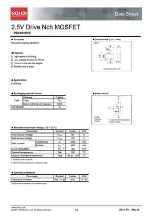
Data Sheet 2.5V Drive Nch MOSFET 2SK3019EB Structure Dimensions (Unit mm) Silicon N-channel MOSFET EMT3F (3) Features 1) High-speed switching. (1) (2) 2) Low voltage drive(2.5V drive). 3) Drive circuits can be simple. 4) Parallel use is easy. Abbreviated symbol KN Application Switching Packaging specifications Inner circuit (3) Package Taping Type ... See More ⇒
7.3. Size:726K mcc
2sk3019.pdf
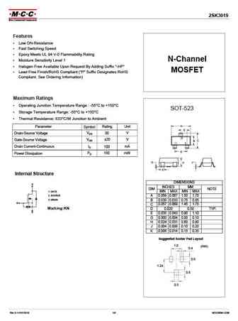
2SK3019 Features Low ON-Resistance Fast Switching Speed Epoxy Meets UL 94 V-0 Flammability Rating Moisture Sensitivity Level 1 N-Channel Halogen Free Available Upon Request By Adding Suffix "-HF" MOSFET Lead Free Finish/RoHS Compliant ("P" Suffix Designates RoHS Compliant. See Ordering Information) Maximum Ratings Operating Junction Temperature Range -55... See More ⇒
7.4. Size:1677K jiangsu
2sk3019.pdf

JIANGSU CHANGJING ELECTRONICS TECHNOLOGY CO., LTD SOT-523 Plastic-Encapsulate MOSFETS 2SK3019 N-channel MOSFET ID V(BR)DSS RDS(on)MAX SOT-523 8 @4V 30V 100mA 13 @2.5V 1. GATE 2. SOURCE 3. DRAIN FEATURE APPLICATION Low on-resistance Interfacing , Switching Fast switching speed Low voltage drive makes this device ideal for Portable equipment Easily des... See More ⇒
7.5. Size:709K wietron
2sk3019t.pdf
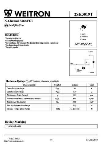
2SK3019T N-Channel MOSFET 3 P b Lead(Pb)-Free 1 2 1. GATE FEATURES 2. SOURCE * Low on-resistance 3. DRAIN * Fast switching speed * Low voltage drive makes this device ideal for portable equipment SOT-523(SC-75) * Easily designed drive circuits * Easy to parallel Maximum Ratings (TA=25 Cunless otherwise specified) Characteristic Symbol Values Unit Drain-Source Voltage VDSS 3... See More ⇒
7.6. Size:485K willas
2sk3019tt1.pdf
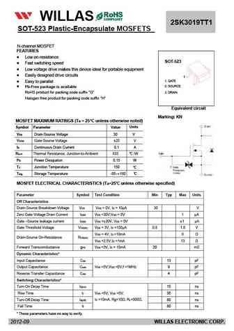
FM120-M WILLAS THRU 2SK3019TT1 SOT-523 Plastic-Encapsulate MOSFETS FM1200-M 1.0A SURFACE MOUNT SCHOTTKY BARRIER RECTIFIERS -20V- 200V SOD-123 PACKAGE Pb Free Product Package outline N-channel MOSFET Features FEATURES Batch process design, excellent power dissipation offers better reverse leakage current and thermal resistance. SOD-123H Low on-resistance Low... See More ⇒
7.7. Size:574K shenzhen
2sk3019.pdf
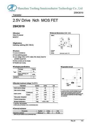
Shenzhen Tuofeng Semiconductor Technology Co., Ltd 2SK3019 Transistor 2.5V Drive Nch MOS FET 2SK3019 External dimensions (Unit mm) Structure Silicon N-channel EMT3 MOSFET 1.6 0.7 0.55 0.3 ( ) 3 Applications ( ) ( ) 2 1 Interfacing, switching (30V, 100mA) 0.2 0.2 0.15 0.5 0.5 1.0 (1)Source Features (2)Gate 1) Low on-resistance. (3)Drain Abbreviated sym... See More ⇒
7.8. Size:320K cystek
2sk3019c3.pdf
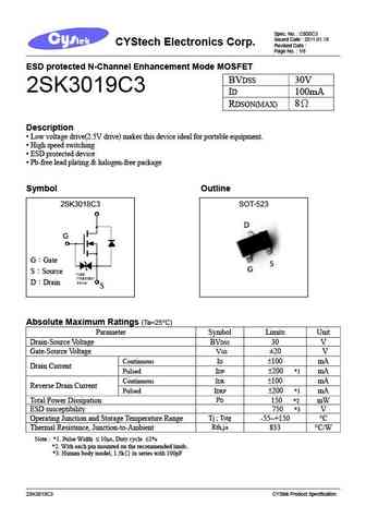
Spec. No. C800C3 Issued Date 2011.01.19 CYStech Electronics Corp. Revised Date Page No. 1/8 ESD protected N-Channel Enhancement Mode MOSFET BVDSS 30V 2SK3019C3 ID 100mA 8 RDSON(MAX) Description Low voltage drive(2.5V drive) makes this device ideal for portable equipment. High speed switching ESD protected device Pb-free lead plating & ha... See More ⇒
7.9. Size:558K lrc
l2sk3019lt1g.pdf
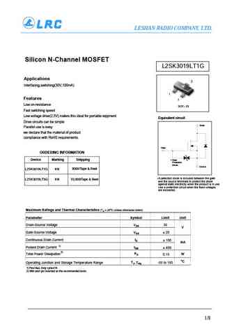
LESHAN RADIO COMPANY, LTD. Silicon N-Channel MOSFET L2SK3019LT1G Applications 3 Interfacing,switching(30V,100mA) 1 Features 2 Low on-resistance SOT 23 Fast switching speed Low voltage drive(2.5V) makes this ideal for portable equipment Equivalent circuit Drive circuits can be simple Drain Parallel use is easy we declare that the material of product compliance with RoHS... See More ⇒
7.10. Size:969K kexin
2sk3019.pdf
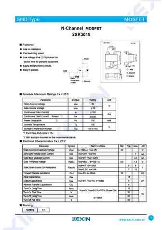
SMD Type MOSFET N-Channel MOSFET 2SK3019 Features Low on-resistance. Fast switching speed. Low voltage drive (2.5V) makes this Drain device ideal for portable equipment. Easily designed drive circuits. 1 Gate Easy to parallel. Gate 2 Source 3 Drain Gate Protection Source Diode Absolute Maximum Ratings Ta = 25 Parameter Symbol Rating Uni... See More ⇒
7.11. Size:1465K cn shikues
2sk3019.pdf
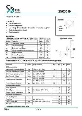
2SK3019 N-channel MOSFET SOT-523 FEATURES 3 Low on-resistance 1 Fast switching speed 1. GATE Low voltage drive makes this device ideal for portable equipment 2 2. SOURCE Easily designed drive circuits 3. DRAIN Easy to parallel Marking KN Equivalent circuit MOSFET MAXIMUM RATINGS (Ta = 25 C unless otherwise noted) Units Symbol Parameter Value VDS D... See More ⇒
7.12. Size:208K cn tak cheong
2sk3019.pdf
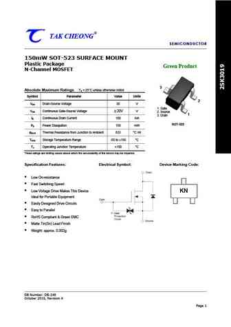
TAK CHEONG SEMICONDUCTOR 150mW SOT-523 SURFACE MOUNT Plastic Package Green Product N-Channel MOSFET 3 Absolute Maximum Ratings TA = 25 C unless otherwise noted Symbol Parameter Value Units 2 VDS Drain-Source Voltage 30 V 1. Gate VGS Continuous Gate-Source Voltage 20V V 2. Source 1 3. Drain ID Continuous Drain Current 100 mA SOT-523 PD Power Dissipation 1... See More ⇒
Detailed specifications: TN0702, TN2106K1-G, TN2106N3-G, TN2524, TP2104K1, TP2104N3, TP2435, 2N7002KWA, K2611, BSS138A, BSS138AKDW, BSS84A, BSS84KW, MCAC10H03, MCAC16N03, MCAC20N15, MCAC30N06Y
Keywords - 2SK3019A MOSFET specs
2SK3019A cross reference
2SK3019A equivalent finder
2SK3019A pdf lookup
2SK3019A substitution
2SK3019A replacement
Can't find your MOSFET?
Learn how to find a substitute transistor by analyzing voltage, current and package compatibility
