FDN5632N-F085 Specs and Replacement
Type Designator: FDN5632N-F085
Type of Transistor: MOSFET
Type of Control Channel: N-Channel
Absolute Maximum Ratings
Pd ⓘ - Maximum Power Dissipation: 1.1 W
|Vds|ⓘ - Maximum Drain-Source Voltage: 60 V
|Vgs|ⓘ - Maximum Gate-Source Voltage: 20 V
|Id| ⓘ - Maximum Drain Current: 1.7 A
Tj ⓘ - Maximum Junction Temperature: 150 °C
Electrical Characteristics
tr ⓘ - Rise Time: 1.7 nS
Cossⓘ - Output Capacitance: 60 pF
RDSonⓘ - Maximum Drain-Source On-State Resistance: 0.082 Ohm
Package: SSOT-3
FDN5632N-F085 substitution
- MOSFET ⓘ Cross-Reference Search
FDN5632N-F085 datasheet
fdn5632n-f085.pdf
ON Semiconductor Is Now To learn more about onsemi , please visit our website at www.onsemi.com onsemi and and other names, marks, and brands are registered and/or common law trademarks of Semiconductor Components Industries, LLC dba onsemi or its affiliates and/or subsidiaries in the United States and/or other countries. onsemi owns the rights to a number of patents, trademarks,... See More ⇒
fdn5632n f085.pdf
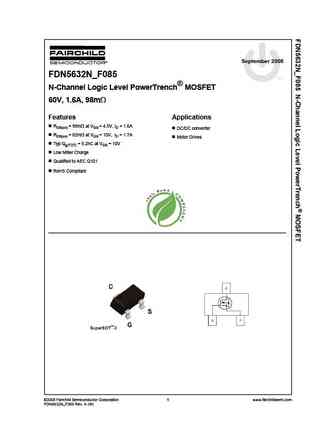
September 2008 FDN5632N_F085 tm N-Channel Logic Level PowerTrench MOSFET 60V, 1.6A, 98m Features Applications RDS(on) = 98m at VGS = 4.5V, ID = 1.6A DC/DC converter RDS(on) = 82m at VGS = 10V, ID = 1.7A Motor Drives Typ Qg(TOT) = 9.2nC at VGS = 10V Low Miller Charge Qualified to AEC Q101 RoHS Compliant 2008 Fairchild Semiconductor Corporation 1 www.fairchild... See More ⇒
fdn5630.pdf
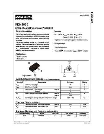
March 2000 FDN5630 60V N-Channel PowerTrench MOSFET General Description Features This N-Channel MOSFET has been designed specifically 1.7 A, 60 V. RDS(ON) = 0.100 @ VGS = 10 V to improve the overall efficiency of DC/DC converters using RDS(ON) = 0.120 @ VGS = 6 V. either synchronous or conventional switching PWM Optimized for use in high frequenc... See More ⇒
fdn5630-3.pdf
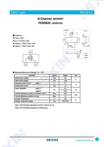
SMD Type MOSFET N-Channel MOSFET FDN5630 (KDN5630) SOT-23-3 Unit mm +0.2 2.9-0.1 +0.1 0.4 -0.1 3 Features VDS (V) = 60V ID = 1.7 A (VGS = 10V) 1 2 RDS(ON) 100m (VGS = 10V) +0.02 +0.1 0.15 -0.02 0.95 -0.1 +0.1 1.9-0.2 RDS(ON) 120m (VGS = 6V) 1. Gate D 2. Source 3. Drain G S Absolute Maximum Ratings Ta = 25 Parameter Symbol Ra... See More ⇒
Detailed specifications: FDMS86368-F085, FDMS86369-F085, FDMS86381-F085, FDMS86581, FDMS8D8N15C, FDMT80040DC, FDN028N20, FDN304P2, IRFP260, FDP030N06B_F102, FDP2710-F085, FDPC3D5N025X9D, FDPC8014AS, FDPF7N50U_G, FDS6898AZ-F085, FDS8449-F085, FDS86267P
Keywords - FDN5632N-F085 MOSFET specs
FDN5632N-F085 cross reference
FDN5632N-F085 equivalent finder
FDN5632N-F085 pdf lookup
FDN5632N-F085 substitution
FDN5632N-F085 replacement
Can't find your MOSFET? Learn how to find a substitute transistor by analyzing voltage, current and package compatibility
🌐 : EN ES РУ
LIST
Last Update
MOSFET: CM4407 | CM3407 | CM3400 | SVF11N65F | SVF11N65T | FKBB3105 | EHBA036R1 | CRTT067N10N | AP6NA3R2MT | AP65SA145DDT8
Popular searches
2sd555 | a950 transistor | k2611 | c1740 transistor | c828 transistor | c4467 | c2383 transistor | 2n3055 equivalent


