NTTFS024N06C Specs and Replacement
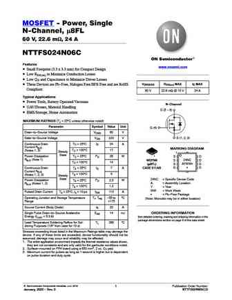
Type Designator: NTTFS024N06C
Type of Transistor: MOSFET
Type of Control Channel: N-Channel
Absolute Maximum Ratings
Pd ⓘ
- Maximum Power Dissipation: 28 W
|Vds|ⓘ - Maximum Drain-Source Voltage: 60 V
|Vgs|ⓘ - Maximum Gate-Source Voltage: 20 V
|Id| ⓘ - Maximum Drain Current: 24 A
Tj ⓘ - Maximum Junction Temperature: 175 °C
Electrical Characteristics
tr ⓘ - Rise Time: 1.3 nS
Cossⓘ -
Output Capacitance: 225 pF
RDSonⓘ - Maximum Drain-Source On-State Resistance: 0.0226 Ohm
Package: WDFN8
NTTFS024N06C substitution
- MOSFET ⓘ Cross-Reference Search
NTTFS024N06C datasheet
..1. Size:141K onsemi
nttfs024n06c.pdf 

MOSFET - Power, Single N-Channel, m8FL 60 V, 22.6 mW, 24 A NTTFS024N06C Features www.onsemi.com Small Footprint (3.3 x 3.3 mm) for Compact Design Low RDS(on) to Minimize Conduction Losses Low QG and Capacitance to Minimize Driver Losses V(BR)DSS RDS(on) MAX ID MAX These Devices are Pb-Free, Halogen Free/BFR Free and are RoHS Compliant 60 V 22.6 mW @ 10 V 24 A Typica... See More ⇒
7.1. Size:198K onsemi
nttfs020n06c.pdf 

MOSFET - Power, Single N-Channel, m8FL 60 V, 20.3 mW, 27 A NTTFS020N06C Features www.onsemi.com Small Footprint (3.3 x 3.3 mm) for Compact Design Low RDS(on) to Minimize Conduction Losses Low QG and Capacitance to Minimize Driver Losses V(BR)DSS RDS(on) MAX ID MAX These Devices are Pb-Free, Halogen Free/BFR Free and are RoHS Compliant 60 V 20.3 mW @ 10 V 27 A Typica... See More ⇒
8.1. Size:205K onsemi
nttfs004n04c.pdf 

NTTFS004N04C MOSFET Power, Single, N-Channel 40 V, 4.9 mW, 77 A Features www.onsemi.com Small Footprint (3.3 x 3.3 mm) for Compact Design Low RDS(on) to Minimize Conduction Losses Low Capacitance to Minimize Driver Losses These Devices are Pb-Free and are RoHS Compliant V(BR)DSS RDS(on) MAX ID MAX 40 V 4.9 mW @ 10 V 77 A MAXIMUM RATINGS (TJ = 25 C unless otherwis... See More ⇒
8.2. Size:201K onsemi
nttfs015p03p8z.pdf 

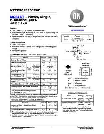
NTTFS015P03P8Z MOSFET Power, Single, P-Channel, m8FL -30 V, 7.5 mW Features www.onsemi.com Ultra Low RDS(on) to Improve System Efficiency Advanced Package Technology in 3.3x3.3mm for Space Saving and Excellent Thermal Conduction V(BR)DSS RDS(on) ID These Devices are Pb-Free, Halogen Free/BFR Free and are RoHS 7.5 mW @ -10 V Compliant -30 V -47.6 A 12 mW @ -4.5 V ... See More ⇒
8.3. Size:193K onsemi
nttfs005n04c.pdf 

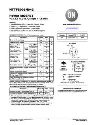
NTTFS005N04C Power MOSFET 40 V, 5.6 mW, 69 A, Single N-Channel Features Small Footprint (3.3 x 3.3 mm) for Compact Design Low RDS(on) to Minimize Conduction Losses www.onsemi.com Low Capacitance to Minimize Driver Losses These Devices are Pb-Free and are RoHS Compliant V(BR)DSS RDS(on) MAX ID MAX MAXIMUM RATINGS (TJ = 25 C unless otherwise noted) Parameter Symbol Val... See More ⇒
8.4. Size:139K onsemi
nttfs016n06c.pdf 

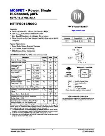
MOSFET - Power, Single N-Channel, m8FL 60 V, 16.3 mW, 32 A NTTFS016N06C Features www.onsemi.com Small Footprint (3.3 x 3.3 mm) for Compact Design Low RDS(on) to Minimize Conduction Losses Low QG and Capacitance to Minimize Driver Losses V(BR)DSS RDS(on) MAX ID MAX These Devices are Pb-Free, Halogen Free/BFR Free and are RoHS Compliant 60 V 16.3 mW @ 10 V 32 A Typica... See More ⇒
8.5. Size:199K onsemi
nttfs030n06c.pdf 

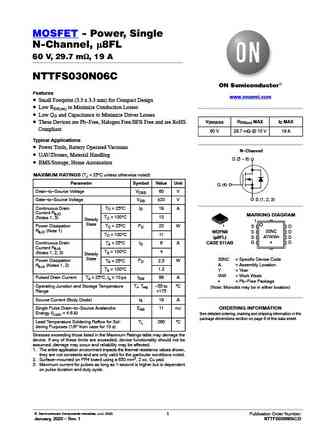
MOSFET - Power, Single N-Channel, m8FL 60 V, 29.7 mW, 19 A NTTFS030N06C Features www.onsemi.com Small Footprint (3.3 x 3.3 mm) for Compact Design Low RDS(on) to Minimize Conduction Losses Low QG and Capacitance to Minimize Driver Losses V(BR)DSS RDS(on) MAX ID MAX These Devices are Pb-Free, Halogen Free/BFR Free and are RoHS Compliant 60 V 29.7 mW @ 10 V 19 A Typica... See More ⇒
8.6. Size:188K onsemi
nttfs008n04c.pdf 

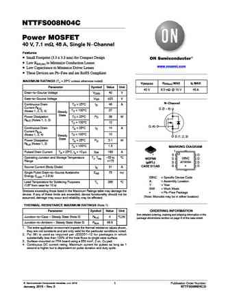
NTTFS008N04C Power MOSFET 40 V, 7.1 mW, 48 A, Single N-Channel Features Small Footprint (3.3 x 3.3 mm) for Compact Design Low RDS(on) to Minimize Conduction Losses www.onsemi.com Low Capacitance to Minimize Driver Losses These Devices are Pb-Free and are RoHS Compliant MAXIMUM RATINGS (TJ = 25 C unless otherwise noted) V(BR)DSS RDS(on) MAX ID MAX Parameter Symbol Val... See More ⇒
8.7. Size:196K onsemi
nttfs003n04c.pdf 

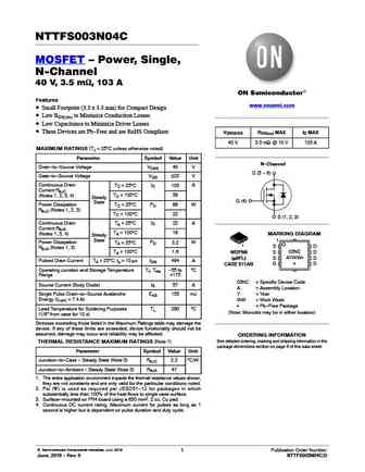
NTTFS003N04C MOSFET Power, Single, N-Channel 40 V, 3.5 mW, 103 A Features www.onsemi.com Small Footprint (3.3 x 3.3 mm) for Compact Design Low RDS(on) to Minimize Conduction Losses Low Capacitance to Minimize Driver Losses These Devices are Pb-Free and are RoHS Compliant V(BR)DSS RDS(on) MAX ID MAX 40 V 3.5 mW @ 10 V 103 A MAXIMUM RATINGS (TJ = 25 C unless otherw... See More ⇒
8.8. Size:199K onsemi
nttfs015n04c.pdf 

NTTFS015N04C MOSFET Power, Single, N-Channel 40 V, 17.3 mW, 27 A Features www.onsemi.com Small Footprint (3.3 x 3.3 mm) for Compact Design Low RDS(on) to Minimize Conduction Losses Low Capacitance to Minimize Driver Losses These Devices are Pb-Free and are RoHS Compliant V(BR)DSS RDS(on) MAX ID MAX 40 V 17.3 mW @ 10 V 27 A MAXIMUM RATINGS (TJ = 25 C unless otherw... See More ⇒
8.9. Size:355K onsemi
nttfs002n04cl.pdf 

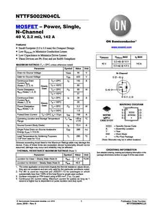
NTTFS002N04CL MOSFET Power, Single, N-Channel 40 V, 2.2 mW, 142 A Features www.onsemi.com Small Footprint (3.3 x 3.3 mm) for Compact Design Low RDS(on) to Minimize Conduction Losses Low Capacitance to Minimize Driver Losses V(BR)DSS RDS(on) MAX ID MAX These Devices are Pb-Free and are RoHS Compliant 2.2 mW @ 10 V 40 V 142 A MAXIMUM RATINGS (TJ = 25 C unless oth... See More ⇒
8.10. Size:387K onsemi
nttfs010n10mcl.pdf 

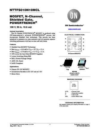
NTTFS010N10MCL MOSFET, N-Channel, Shielded Gate, POWERTRENCH) 100 V, 50 A, 10.6 mW www.onsemi.com General Description This N-Channel POWETRENCH MOSFET is produced using ELECTRICAL CONNECTION ON Semiconductor s advanced POWERTRENCH process that incorporates Shielded Gate technology. This process has been S D optimized to minimize on-state resistance and yet maintain superior ... See More ⇒
8.11. Size:272K onsemi
nttfs002n04c.pdf 

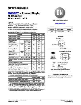
NTTFS002N04C MOSFET Power, Single, N-Channel 40 V, 2.4 mW, 136 A Features www.onsemi.com Small Footprint (3.3 x 3.3 mm) for Compact Design Low RDS(on) to Minimize Conduction Losses Low Capacitance to Minimize Driver Losses These Devices are Pb-Free and are RoHS Compliant V(BR)DSS RDS(on) MAX ID MAX 40 V 2.4 mW @ 10 V 136 A MAXIMUM RATINGS (TJ = 25 C unless other... See More ⇒
Detailed specifications: NTTFS004N04C, NTTFS005N04C, NTTFS008N04C, NTTFS010N10MCL, NTTFS015N04C, NTTFS015P03P8Z, NTTFS016N06C, NTTFS020N06C, 18N50, NTTFS030N06C, NTTFS1D2N02P1E, NTTFS2D8N04HL, NTTFS4C02N, NTTFS5C453NL, NTTFS5C454NL, NTTFS5C460NL, NTTFS5C466NL
Keywords - NTTFS024N06C MOSFET specs
NTTFS024N06C cross reference
NTTFS024N06C equivalent finder
NTTFS024N06C pdf lookup
NTTFS024N06C substitution
NTTFS024N06C replacement
Learn how to find the right MOSFET substitute. A guide to cross-reference, check specs and replace MOSFETs in your circuits.
